


ON Semiconductor Launches CCD Image Sensor
 Published2015.11.20 12:43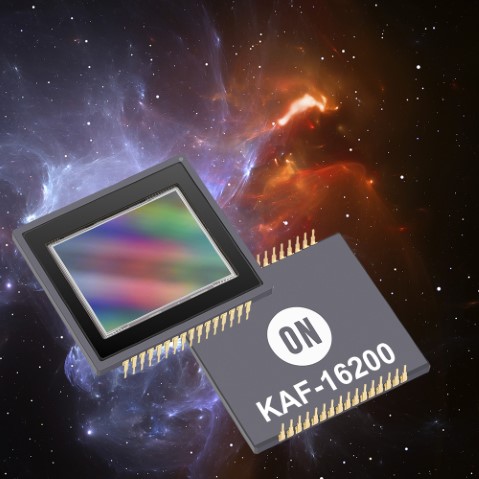
Advancement of image capture technology to meet astrophotography and scientific imaging applications
ON Semiconductor announced that it has taken image capture technology to the next level by launching a new 16.2-megapixel (MP) charge-coupled device (CCD) image sensor to meet astrophotography and scientific imaging applications.
The newly released KAF-16200 CCD image sensor enables high-quality image capture through ON Semiconductor's advanced design and manufacturing technology. The Full Frame CCD architecture adopted in this device provides best-in-class image uniformity and dark current, and uses transparent gate electrodes of 6.0 micrometer (µm) pixels to integrate high sensitivity, high contrast ratio, and an oversaturation preventer.
With such technical excellence, the KAF-16200 provides fine image details through outstanding imaging and the APS-H (34.6mm oblique) optical format.
Herb Erhardt, Head of the Image Sensor Group at ON Semiconductor, said, “This new image sensor offers significant technical advantages to our camera manufacturer customers. The KAF-16200 doubles the resolution compared to our existing devices without compromising CCD-grade image quality when applied to applications. This demonstrates that ON Semiconductor is well-equipped to provide the highest quality image sensors while maintaining existing technology.”
The KAF-16200 is provided in a CERDIP package compliant with RoHS requirements and is available in both black and white and color versions.
Comments
Related news

ON Semiconductor Expands to Sub-1 Gigahertz (GHz) RF Band
ON Semiconductor expanded its wireless portfolio to include sub-1 gigahertz (GHz) RF devices through the acquisition of AXSEM. These devices enabling wireless connectivity support advanced features in IoT, automatic meter reading, home automation, sensor networks, as well as the satellite communications market.
2015.11.04by

ON Semiconductor Strengthens Development of IoT Innovation Products
ON Semiconductor has launched IoT solutions leveraging the Intel® Quark™ processor family for diverse IoT applications.
2015.11.09by

Intel Unveils Next-Generation 'Core Ultra Series 3' and vPro Platform for Enterprise PCs
Intel has officially unveiled the "Intel Core Ultra Series 3" for next-generation enterprise PCs and the latest vPro platform, addressing a wide range of demands from enterprise notebooks to high-performance workstations.
2026.03.26by 배종인 기자

ROHM Launches ESD Protection Diode Compatible with High-Speed Interfaces of 10Gbps or Higher
Semiconductor specialist ROHM has developed the 'RESDxVx series' of ESD (electrostatic discharge) protection diodes capable of responding to next-generation high-speed data communication environments exceeding 10Gbps, simultaneously enhancing both signal quality maintenance required in high-speed interfaces and IC protection performance.
2026.03.26by 배종인 기자











