



ON Semiconductor and Hexius Collaborate to Validate Analog IP Blocks
 Published2017.01.11 11:35
Reduce development cycle risk and rework risks by providing new IPs.
ON Semiconductor announced a collaboration with Hexius Semiconductor, a specialist in IP development for analog ICs, to verify several analog IP blocks in its ONC18 0.18 µm CMOS process.
ON Semiconductor stated that the eight initial designs, developed through this collaboration, include a variety of ADCs, DACs, voltage and current references, and can be customized to meet specific application requirements. IP for data converter and PLL designs is currently under development, with release planned for the second half of this year.
Additionally, ON Semiconductor's ONC18 process is said to be suitable for automotive, industrial, military, and medical development due to its high-voltage capacity based on a 0.18 micrometer (µm) CMOS architecture.
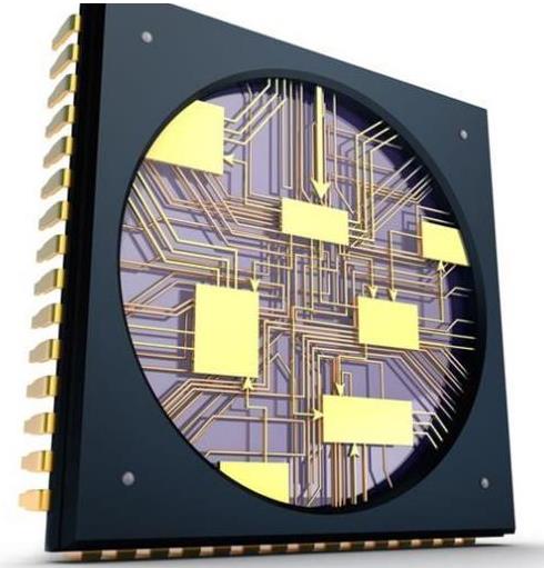
▲Capture from Hexius Semiconductor homepage.
Customers have access to a broad portfolio of IP supporting this process, allowing them to benefit from ASIC implementations optimized for their specific requirements without having to dedicate significant in-house engineering resources to the task. This results in faster design cycles and reduced risk of rework.
“The mixed-signal ASIC market continues to grow as systems increasingly need to leverage real-world data captured by sensors and user interfaces,” said Rocke Acree, director of the Custom Foundry business unit at ON Semiconductor. “OEMs want to integrate more efficient proprietary designs rather than relying on standard off-the-shelf components or silicon, which can boost performance while saving board space and significantly reducing unit cost. Working together, our companies will enable new mixed-signal designs by providing proven analog IP that facilitates this.”
Comments
Related news
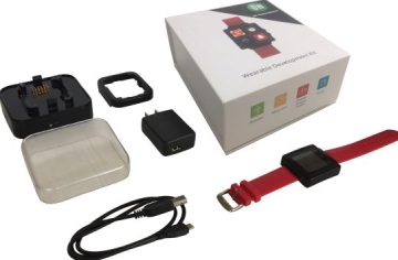
Onsemi Unveils Scalable Design Platform for Next-Generation Wearable Devices
ON Semiconductor has introduced comprehensive development resources targeting wearable electronics, utilizing diverse semiconductor technologies including analog, power management, sensor interfaces, and signal conditioning. The newly launched Wearable Development Kit (WDK 1.0) is composed of multiple highly optimized components designed to support OEM companies seeking to bring differentiated products to market. By utilizing this kit, developers can significantly accelerate the design cycle of wearable electronic products while reducing engineering costs.
2016.12.06by 신윤오 기자

ON Semi Unveils USB Type-C Solution at CES 2017
ON Semiconductor plans to launch a comprehensive solution portfolio for effective implementation of USB Type-C applications at the 2017 International Consumer Electronics Show (CES 2017) in Las Vegas. USB Type-C is emerging rapidly as an industry standard for wired smart connectivity, fast charging, and high-speed data transmission, supporting applications such as high-resolution video and augmented and virtual reality. The underlying USB 3.1 protocol can theoretically achieve maximum data speeds of up to 10Gbps, which is twice as fast as USB 3.0, and this is critical in ensuring the operation of portable devices that maintain continuous connectivity and reliably perform their functions.
2016.12.22by 신윤오 기자

Intel Unveils Next-Generation 'Core Ultra Series 3' and vPro Platform for Enterprise PCs
Intel has officially unveiled the "Intel Core Ultra Series 3" for next-generation enterprise PCs and the latest vPro platform, addressing a wide range of demands from enterprise notebooks to high-performance workstations.
2026.03.26by 배종인 기자

ROHM Launches ESD Protection Diode Compatible with High-Speed Interfaces of 10Gbps or Higher
Semiconductor specialist ROHM has developed the 'RESDxVx series' of ESD (electrostatic discharge) protection diodes capable of responding to next-generation high-speed data communication environments exceeding 10Gbps, simultaneously enhancing both signal quality maintenance required in high-speed interfaces and IC protection performance.
2026.03.26by 배종인 기자

ST Launches 75V Drive IC Targeting 48V Industrial Motor Driving
ST Microelectronics has unveiled the 'STSPIN9P' series of 75V motor drive ICs tailored for 48V-class industrial drive system design. The new product family is characterized by half-bridge and full-bridge configurations that enable design scalability according to motor type and output conditions. Power supply circuits, protection functions, and current sensing circuits are integrated on-chip to simplify system configuration, and the devices are designed to support applications up to 500W maximum. The company plans to provide reference designs and demo boards to support development and evaluation in industrial automation, robotics, pumps, fans, lighting, and textile machinery.
2026.03.26by 배종인 기자











