


Image sensor capable of capturing images quickly or slowly
 Published2017.03.23 18:02
When designing an image sensor, the most important step is to fully understand how the device is used. You must explain to customers how to operate the product equipped with the device.
There is an endless array of questions customers ask, such as whether they want to use the device primarily in high frame rates or low-light environments, or if they want to optimize it for low power or low read noise. While it is natural for a finished product to be used in more than one way, complications can arise if the intended applications for a new product contradict the intended design direction.
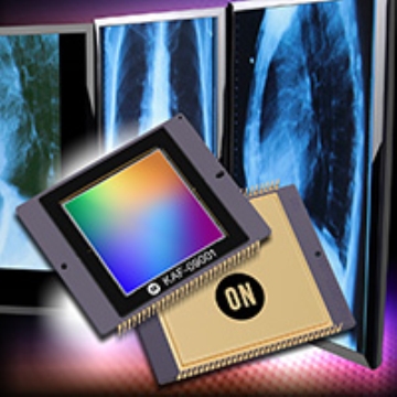
Taking ON Semiconductor’s recently released KAL-09001 image sensor as an example, like the existing KAF-09000, this full-frame CCD provides the high quality required to capture images in digital radiology systems. Both devices offer a 9-megapixel resolution in a 12-micron pixel size, providing high sensitivity, high dynamic range, and low image distortion capabilities that allow for the capture of critical details while limiting X-ray exposure.
However, the KAF-09001 can support additional use cases. Specifically, it provides a high-sensitivity video mode that verifies the patient's position before the digital radiology system performs the final high-resolution capture. This increases the sensitivity of the element even with (relatively) short exposure times, providing information in real time and resulting in improved data reading speed.
At first glance, these two use cases seem complex. To maintain low readout speeds, users want this device to operate at low speeds, but very high speeds are required to support video mode. Additionally, pixel size must be increased to achieve sufficient light sensitivity to support video mode. To this end, the number of pixels must be reduced as much as possible for final image capture, or the price must be increased.
To address this, more creative technology was required. Therefore, ON Semiconductor first increased the device's output from one to four to boost speed without altering the existing low-noise amplification design. Additionally, the horizontal register charge capacitance of the CCD was modified to support an increase in the maximum horizontal clock speed. As a result, the device provides additional bandwidth when operating in video mode while still operating at low speeds.
Finally, the number of pixels was slightly adjusted to optimize the new element for both 2 x 2 and 3 x 3 binning, while not only improving imaging sensitivity but also reducing data transfer for video mode.
As a result, a highly diverse and flexible image sensor with various reading options was made possible. For video imaging, pixels can be stored, and as the sensor operates at maximum speed, a 1-megapixel image stream is generated at a rate of up to 10 frames per second.
If the final image needs to be loaded, output speed can be reduced by turning off binning. Therefore, for this application, it has become possible to capture full-resolution images with low distortion while preserving important details.
In other words, this solution is an image sensor optimized for two use cases according to a doctor's instructions.
(Source: ON Semiconductor Blog, by Michael DeLuca)
Comments
Related news
ON Semiconductor Image Sensors Provide Enhanced Output Capabilities at No Additional Cost
ON Semiconductor has launched a CCD image sensor that produces video images with minimal X-ray exposure. The solution minimizes X-ray exposure during radiography, enhancing patient safety. The newly released KAF-09001 image sensor features the same high-sensitivity, low-noise 12-micron pixel as the existing KAF-09000 model used in digital radiography. In addition to this, it includes output for high-sensitivity video mode, providing full-resolution frame rates increased by up to 10 times.
2017.03.08by 김자영 기자
Digi-Key Named a Global Outstanding Service Provider for ON Semiconductor
Recently, ON Semiconductor selected Digi-Key Electronics, a global electronic components distributor, as the recipient of the '2016 Global High Service Distributor Award'.
2017.03.09by 신윤오 기자

ONSemi Releases Latest Version of IoT Development Kit
ON Semiconductor has released the latest version of its Internet of Things (IoT) development kit. This multifaceted product with a unique modular structure composed of hardware and software is a platform designed to help engineers test and develop differentiated IoT systems in the shortest timeframe and quickly bring them to market.
2017.03.17by 김자영 기자

Intel Unveils Next-Generation 'Core Ultra Series 3' and vPro Platform for Enterprise PCs
Intel has officially unveiled the "Intel Core Ultra Series 3" for next-generation enterprise PCs and the latest vPro platform, addressing a wide range of demands from enterprise notebooks to high-performance workstations.
2026.03.26by 배종인 기자

ROHM Launches ESD Protection Diode Compatible with High-Speed Interfaces of 10Gbps or Higher
Semiconductor specialist ROHM has developed the 'RESDxVx series' of ESD (electrostatic discharge) protection diodes capable of responding to next-generation high-speed data communication environments exceeding 10Gbps, simultaneously enhancing both signal quality maintenance required in high-speed interfaces and IC protection performance.
2026.03.26by 배종인 기자











