


ADI Launches SAR ADC with Built-in Picoampere Input Buffer
 Published2017.04.18 14:34
Direct sensor connection without loss of measurement accuracy due to CMRR characteristics
Analog Devices announced the release of the new LTC2358-18, an 18-bit, 8-channel simultaneous sampling SAR (successive approximation register) ADC with a built-in picoampere (pA) input buffer.
Particularly when board space is limited, the LTC2358-18 reduces space and cost by eliminating the front-end signal conditioning circuitry commonly required to drive buffered switched-capacitor ADC inputs. By saving three amplifiers, six resistors, and two capacitors per channel, a total of 88 components can be reduced across eight channels. This not only significantly reduces board area and bill of materials (BOM) costs but also provides a reduction in power consumption of over 40%.
Due to its picoampere input and 128dB CMRR characteristics over a 30V PP common mode range, the LTC2358-18 can be directly connected to various sensors without compromising measurement accuracy.
The LTC2358-18 converts 8 channels with a throughput of 200 ksps per channel, and offers greater flexibility through an individually configurable SoftSpan™ input range. Each channel can be programmed on a conversion-by-conversion basis to accept ±10.24V, 0V to 10.24V, ±5.12V, or 0V to 5.12V unipolar, true bipolar, fully differential, or arbitrary input signals.
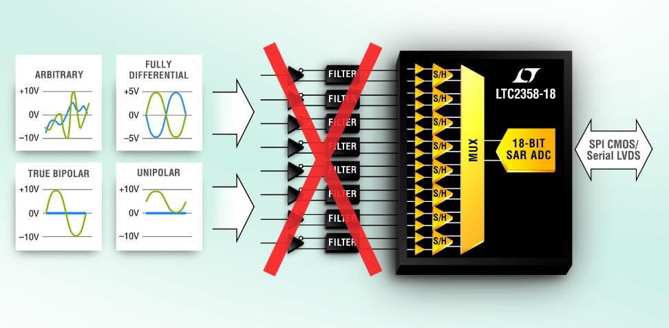
The differential analog input operates over a wide input common-mode range of 30V, allowing this ADC to directly convert various signals into digital while simplifying signal chain design. Combined with such input signal flexibility and excellent characteristics such as a maximum INL of ±3.5 LSB, no code loss at 18 bits, and 96.4 dB SNR, the LTC2358-18 is ideal for high-performance industrial process control, test and measurement, power line monitoring, and motor control applications.
The LTC2358-18 features a precision internal reference supporting a maximum temperature factor of 20 ppm/ ° C and an integrated reference buffer capable of precise one-shot measurements, providing space-saving benefits for densely packaged circuit boards. An optional external 5V reference can be used to extend the analog input range to ±12.5V. The device consumes 219 mW of power when converting eight channels simultaneously at 200 ksps per channel and offers nap and power-down modes to reduce heat dissipation at slower throughputs.
In addition to its unique analog characteristics, the LTC2358-18 offers excellent digital flexibility featuring pin-selectable SPI CMOS and LVDS serial interfaces. With a wide digital output power range, it can communicate with any CMOS logic between 1.8V and 5V. In CMOS mode, applications can select from 1 to 8 lanes of serial output data, allowing users to optimize bus width and data throughput. LVDS mode uses differential signaling to provide low-noise, high-speed communication over longer distances. In addition, these I/O interface options enable the LTC2358-18 to communicate on par with legacy microcontrollers (MCUs) and modern FPGAs.
Comments
Related news

ADI Collaborates with Renesas Electronics on RADAR Technology
Analog Devices announced that it will collaborate with Renesas Electronics in the field of system-level 77/79-GHz RADAR sensor test equipment for enhancing ADAS applications and implementing autonomous vehicles.
2017.04.13by 김자영 기자
ADI Launches Step-Down Regulator Meeting CISPR 22 Class B Requirements
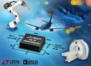
Analog Devices has launched the LTM8073, a μModule® step-down regulator that supports input voltage ranges up to 60V (65V absolute maximum). This regulator can safely operate in noisy environments such as telecommunications infrastructure, factory automation, industrial robotics, and aviation systems, utilizing unregulated or variable 24V to 48V input voltages.
2017.04.13by 김지혜 기자
ADI Launches Regulator Based on Silent Switcher 2 Architecture
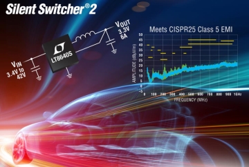
Analog Devices announced the launch of LT8640S, a new synchronous step-down switching regulator that supports 6A output and 42V input. The product features Silent Switcher® 2 architecture. It is characterized by the use of two internal input capacitors, as well as internal BST and INTVCC capacitors to minimize hot loop area.
2017.04.17by 김지혜 기자

Intel Unveils Next-Generation 'Core Ultra Series 3' and vPro Platform for Enterprise PCs
Intel has officially unveiled the "Intel Core Ultra Series 3" for next-generation enterprise PCs and the latest vPro platform, addressing a wide range of demands from enterprise notebooks to high-performance workstations.
2026.03.26by 배종인 기자

ROHM Launches ESD Protection Diode Compatible with High-Speed Interfaces of 10Gbps or Higher
Semiconductor specialist ROHM has developed the 'RESDxVx series' of ESD (electrostatic discharge) protection diodes capable of responding to next-generation high-speed data communication environments exceeding 10Gbps, simultaneously enhancing both signal quality maintenance required in high-speed interfaces and IC protection performance.
2026.03.26by 배종인 기자











