



KETI Provides Technological Support to SMEs with Core Advanced Electronic Materials Technologies
 Published2017.10.10 12:13
A venue was set up to introduce key technologies in the field of advanced electronic materials and components, such as smart patches used in body-attached wearable devices and photo-sintered inks capable of printing circuits for smart devices.
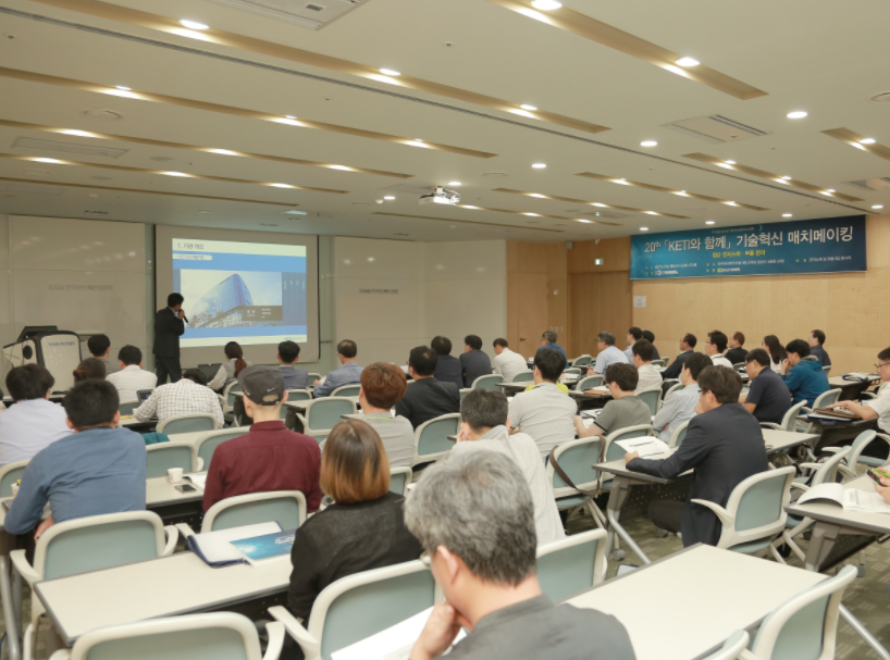
The Electronics Technology Institute (KETI) held a 'Technology Innovation Matchmaking' event at the Korea Semiconductor Industry Center in Pangyo on the 28th. As part of its corporate cooperation platform, the event supports the identification of potential customers, technology transfer, and commercialization to promote the commercialization of public technologies. This regularly held event marked its 20th anniversary.
President Park Cheong-won stated, “I hope that companies in practical need of technology will participate and benefit,” adding, “KETI is not only developing technologies for next-generation growth engines but also securing core technologies for advanced electronic materials and components necessary to realize them.” "We will focus on providing technical support to help our small and medium-sized enterprises (SMEs) and middle-sized companies secure technological competitiveness and grow into global specialized enterprises," he said.
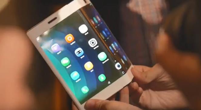
Kim Jun-cheol, Director of the ICT Device Packaging Research Center, explained, “As healthcare and body-worn smart devices combine, they are becoming the mainstream trend in the wearable market. It is expected to become a market worth approximately 5 trillion won by 2020.”
Currently available body-attached wearable devices on the market are worn rather than attached to the skin, which causes inconvenience due to the device's thickness or lack of elasticity. Products designed to address these issues by attaching to the body are expensive, difficult to remove once attached, and difficult to monitor in real time because they rely on NFC for power supply.
KETI selected a method of separating the sensor patch and the power and communication module. The sensor patch is used as a flexible component on a flexible circuit board, while the power and communication module is attached to a non-flexible board. Since the sensor patch is disposable and the communication module is reusable, commercially available components can be used without expensive manufacturing processes, resulting in a lower cost. It can also resolve the difficulty of determining whether a device can be reused after being removed once attached.
The nano-carbon heating material introduced by Principal Researcher Kim Yun-jin of the Nano Materials & Components Research Center offers rapid heating and generates high output from a small surface area. It can reach temperatures up to 300 degrees Celsius across all physical properties and possesses the adhesive properties of paints. Furthermore, it is unaffected by the substrate used for coating, allowing for high design freedom. While high heat resistance typically leads to reduced flexibility, this issue has been resolved to ensure flexibility. The technology is now at a stage where mass production is feasible.
The part of a building with the greatest energy loss is the windows. Accordingly, technology has been introduced to reduce heat loss through windows. Technologies currently on the market include smart windows utilizing thermochromic and electrochromic technologies. KETI has developed an intelligent smart window that combines existing electrochromic and thermochromic technologies to selectively control the window based on the incoming electric field and ambient temperature.
The Smart Sensor Research Center showcased custom MEMS pressure sensors, 3D touch sensor panels, and LiDAR. The application-specific MEMS pressure sensors, manufactured using semiconductor batch manufacturing technology, feature core technologies that offer diverse pressure and wide operating temperature ranges, as well as resistance to high pressure and corrosion. They can be packaged in various forms, including metal, plastic, and ceramic.
The 3D touch sensor panel is a method capable of simultaneously detecting the touch location and force intensity, rather than an indirect method. 5-inch and 10-inch products are currently under development. The LiDAR is a 360-degree scanning multi-channel module that simplifies the optical system by reducing the number of lenses used. Since multi-channel operation is possible through a single lens, miniaturization is feasible and channel expansion is easy. We have successfully commercialized a PLD light source for LiDAR.
Jeong Gu-jin, a principal researcher at the Next-Generation Battery Research Center, explained silicon anode material technology. Since conventional lithium-ion batteries are based on graphite, there are limitations to their energy density, which allows for small size, light weight, and long usage. Consequently, the development of new anode and cathode materials is necessary.
Accordingly, silicon anode materials were produced using three technologies: sol-gel manufacturing technology, porous manufacturing technology, and composite manufacturing technology. Researcher Jeong stated, “These technologies are methods to reduce process costs and improve yield. They facilitate mass production and enable the realization of various nanostructures, which can improve battery characteristics such as capacity, lifespan, and expansion.”
The Display Materials & Components Research Center has developed a transparent electrode with flexible properties. Transparent electrodes are utilized in public displays, wearable devices, quantum dot materials, and optical application technologies. A flexible transparent electrode is a thin-film conductor that imparts electrical conductivity while maintaining transparency on the surface of a flexible transparent insulator, such as a plastic film or a highly elastic transparent insulator like PDMS.
By fabricating transparent electrodes based on ITO nanoparticles, it is possible to apply them to flexible substrates while reducing the usage of ITO, an expensive rare metal (indium-tin oxide) that is currently dependent on imports. The hybrid structure of an ITO-NPs layer and a silver nanowire layer minimizes changes in electrode resistance. It demonstrates advantages in durability, flexibility, and thermal stability.
Senior Researcher Hong Seong-je, who introduced the technology, stated, “This technology can be used in displays, touch sensors, OPVs, and transparent heaters,” adding, “Silver nanowires and metal mesh will be dominant in the industry going forward.”
Comments
Related news
The Slow Popularization of VR/AR Can Be Found in Convergence Technology
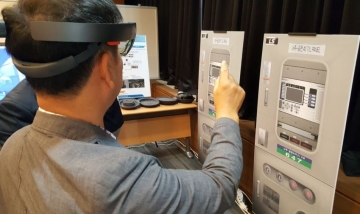
A venue has been established to view at a glance the current state of VR and AR technologies as well as hologram technology. This is the 15th Technology Innovation Matchmaking event hosted by KETI, which connects technologies developed with small and medium-sized enterprises. The Electronics and Telecommunications Research Institute (KETI) introduced nine related technologies: ▲hologram printing ▲experiential sportainment VR ▲power facility visualization using VR/AR ▲virtual training collaborative platform ▲non-contact NUI/NUX ▲3D convergence performance evaluation and VR/AR demonstration technology ▲3D virtual digital manufacturing. Various technologies were demonstrated, including a device that appears as a VR driving game, TVs, and ski VR equipment. The first technology that caught attention was the 'smart substation' technology that KETI jointly developed with Korea Electric Power Corporation in February. It can 3D scan from basement level 1 to above-ground floor 3 and view the modeled facility environment in real-time AR.
2017.05.15by 김자영 기자
Upgraded IoT Platform Mobius, Will Global Commercialization Expand?
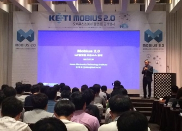
Where is the Internet of Things (IoT) heading in its evolution? Mobius 2.0, an upgraded version of the Internet of Things platform developed by the Electronics and Telecommunications Research Institute (KETI), has been unveiled. Mobius is a platform operated as open source with source code publicly disclosed, created based on oneM2M, a global IoT standard. KETI held an event introducing Mobius 2.0 at Elltower in Yangjae on the 20th. Since first introducing Mobius 1.0 in 2015, the upgraded version was released based on developers' requirements. Park Chung-won, President of KETI, said, "We started from a time when IoT wasn't receiving much attention, and today we're unveiling the 2.0 version. As we move toward a hyper-connected society, interoperability between devices becomes important, and Mobius has technological competitiveness in that regard."
2017.07.21by 김지혜 기자
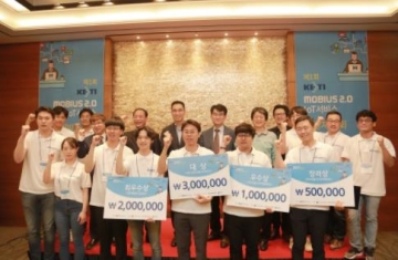
KETI Holds Mobius 2.0 IoT Service Excellence Awards Ceremony
The first KETI Mobius 2.0 IoT Service Developer Competition, which began last July, has come to a close. KETI held an awards ceremony on the 27th after conducting final judging for 13 teams that advanced to the finals and presenting prizes for outstanding works. Mobius, developed by KETI, is the world's first open-source IoT platform developed based on oneM2M, a representative IoT standard. It leads international standardization efforts and boasts world-class compatibility, while featuring high openness and enabling easy and convenient development.
2017.09.29by 김지혜 기자
ESP32 Development Environment Selection and GPS Application Implementation
The ESP32 is a microcontroller that integrates Wi-Fi, Bluetooth, 12-bit ADC, capacitive touch, PWM, DAC, and UART in a single SoC. However, the abundance of features does not by itself solve the designer's problems. The real challenges lie in selecting the appropriate development environment, determining which pins can be used and which must be avoided, and converting raw data from modules into usable information. This document addresses ESP32 peripheral constraints (ADC2 and Wi-Fi coexistence limitation, UART1 occupancy, ADC non-linear regions), the trade-offs between Arduino IDE and ESP-IDF, and the process from connecting NEO-6M/NEO-M8N GPS modules to UART2, parsing NMEA sentences, and visualizing routes in Google Earth, all organized based on documented references.
2026.10.12by 편집부
MIPI CSI-2, DSI-2, C-PHY, D-PHY Test Solution Technical White Paper
The MIPI interface adopts a burst mode that transitions between low-power (LP) and high-speed (HS) states for low-power consumption, and in return, strict timing rules are imposed on state transitions. Additionally, the high-speed section operates as a packet-based protocol with headers, ECC, and CRC, so verification engineers must handle waveforms and protocols simultaneously. Traditional configurations combining general-purpose oscilloscopes and AWGs reveal limitations in setup complexity, measurement uncertainty, and lack of reproducibility when faced with these requirements. This white paper, based on webinar materials, organizes the structure of this problem and describes how the SV5C-DPTXCPTX generator for receiver testing and SV5C-DPRXCPRX analyzer for transmitter testing integrate state transition testing, stressed eye testing, and protocol analysis into a single bench, along with their application boundaries.
2026.10.12by 편집부











