



ON Semiconductor Unveils Scalable Image Sensor for Autonomous Driving
 Published2018.01.09 10:25
ON Semiconductor, driving energy efficient innovations, has announced a scalable family of CMOS image sensors ideal for a wide range of applications related to Advanced Driver Assistance Systems (ADAS) and autonomous driving. This new sensor family, based on a common platform and feature set, enables automakers and tier-one suppliers to design powerful imaging devices.
ON Semiconductor's new sensors range in resolution from 1.2 megapixels (MP) to 8.3 MP, and feature large 4.2 µm pixels for industry-leading low-light performance. Additional features include functional safety up to ASIL-C, high-dynamic range (HDR), an industry-first cybersecurity option, and second-generation wafer stacking technology that reduces package size. Multiple technology partners are currently testing individual products within this platform, and Mobileye and NVIDIA are testing compatibility with their DRIVE AI computing platform for autonomous vehicles.
The scalable image sensor family, supporting a variety of resolutions suitable for next-generation ADAS and autonomous driving systems, includes the AR0820AT, AR0220AT, and AR0138AT. Automakers require a variety of resolutions depending on the product line, which includes specific safety features as standard. However, by adding cameras or using higher resolution cameras, we can provide our customers with improved safety and advanced features.
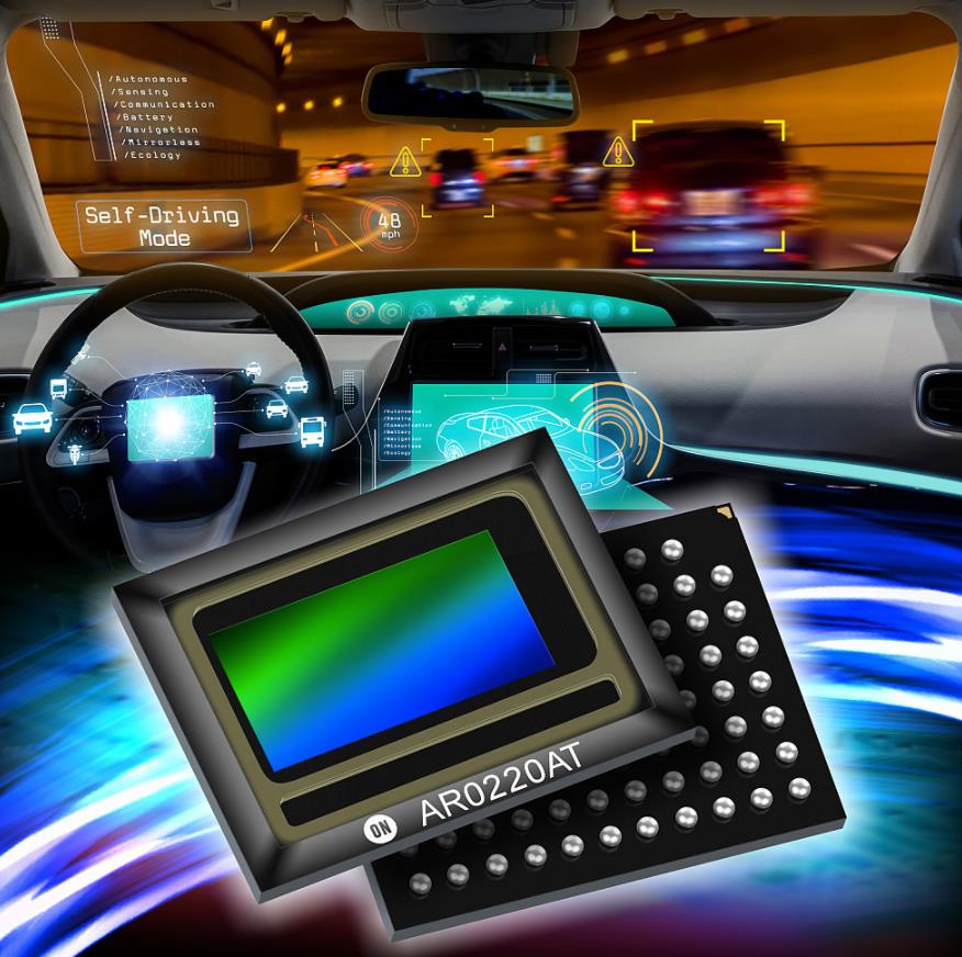
As the automotive industry moves from Level 2 systems like standard Autonomous Emergency Braking (AEB), Adaptive Cruise Control (ACC), and Lane Change Assist (LCA) to fully autonomous driving, ON Semiconductor's image sensors enable advanced ADAS and autonomous driving capabilities. Furthermore, their large 4.2 µm pixels deliver leading performance in low-light environments, including night-time emergency braking for pedestrians and cyclists – a safety requirement for Euro NCAP (European Car Assessment Program). Furthermore, the new image sensor family's cybersecurity technology ensures reliable and secure operation when multiple cameras around the vehicle are connected to a central system where data and commands are relayed via wires between the sensors and processors.
For advanced imaging capabilities, software and algorithm testing are the most time-consuming tasks during the development phase. Leveraging ON Semiconductor's scalable image sensor portfolio, customers can begin initial development with a single sensor, tailoring algorithms to pixel performance and system capabilities, and then expand resolution through additional testing. This will shorten the project time and reduce the overall development costs associated with building a camera system.
“As the number of image sensors on a vehicle increases, having a scalable platform with common core technologies and pixel architecture will enable automakers to deliver new safety and autonomous driving features faster and more efficiently,” said Ross Jatou, vice president and general manager of the Automotive Solutions Division at ON Semiconductor. “We are committed to engaging closely with our customers and leveraging the advanced capabilities of our new image sensor family to empower them in their ADAS and autonomous driving program development efforts.”
ON Semiconductor will showcase its new scalable image sensor portfolio, along with a range of advanced semiconductor-based products, including automotive solutions, at CES 2018. ON Semiconductor imaging experts will be on-site throughout the event to answer questions about solutions for automotive image sensor applications. ON Semiconductor's booth will be located at the Sands Convention Center or the Venetian Hotel (Murano 3302).
Comments
Related news

ON Semiconductor Supplies Image Sensors for ADAS to Bosch
ON Semiconductor announced that Bosch has selected ON Semiconductor, a global leader in automotive image sensor technology, as an image sensor supplier for future camera technology for Advanced Driver Assistance Systems (ADAS). The new image sensor, designed to meet OEM requirements for future ADAS cameras, delivers high dynamic range (HDR) with state-of-the-art functional safety features.
2017.11.13by 김지혜 기자

ON Semiconductor Unveils Automotive Electronic Content Technology at CES 2018
ON Semiconductor showcases technologies at CES 2018 in Las Vegas that enable advances toward fully autonomous driving and increased electronic content in connected vehicles. Visitors can easily understand the latest technology trends through ON Semiconductor's exhibits. During the event, visitors will experience ON Semiconductor's latest image sensor solutions for various advanced driver assistance systems (ADAS) applications such as forward view, surround view, rear view, and driver monitoring through a demonstration of the automotive image sensing application platform. ON Semiconductor's image sensors meet all requirements including resolution and clarity for Level 3 or higher autonomous driving, as well as robust image capture in low light conditions.
2017.12.27by 김지혜 기자

ON Semiconductor Joins the International Electric Vehicle Charging Association to Develop EV Charging Standards
ON Semiconductor announced its membership in CharIN (Charging Interface Initiative e.V.), an international electric vehicle charging association. CharIN is an international association that aims to establish standards for electric vehicle charging systems, define requirements necessary for the advancement of electric vehicle charging systems, and develop certification systems needed for manufacturers to implement charging systems in their products. ON Semiconductor possesses all core technologies for electric vehicles. In particular, it has a comprehensive portfolio of vehicle-certified power management products, including insulated gate bipolar transistors (IGBTs), high-voltage gate drivers, super junction rectifiers, high-voltage MOSFETs, high-voltage DC-DC converters, and wide band gap semiconductor devices made of silicon carbide (SiC) and gallium nitride (GaN) materials.
2018.01.08by 김지혜 기자
[e4ds Tech Day 2026 ⑨] Sim Sang-gyu, Autocrypt CTO: "In the Physical AI Era, Automotive Security Must Extend Beyond the Vehicle"
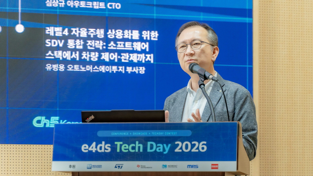
At e4ds Tech Day 2026, Sim Sang-gyu, CTO of Autocrypt, explained automotive cybersecurity strategies in the era of Physical AI and SDV (Software-Defined Vehicle). Automobiles are evolving as part of an ecosystem connected to AI, cloud, chargers, IoT, and robots, and he emphasized that the scope of security must expand beyond the vehicle interior to the entire connected environment. In particular, AI model tampering, adversarial attacks, OTA updates, and EV charger hacking were identified as major threats. He explained that response measures require zero trust, AI model integrity protection, intrusion detection, Security by Design and Default, and full lifecycle security management, and that proactive security system establishment beyond regulatory compliance is critical for securing future mobility competitiveness.
2026.10.12by 배종인 기자

Practical HIL Construction Strategy for Automotive and Off-Highway Controller Validation
As vehicle E/E architecture transitions to zonal structures and shifts to software-defined vehicles (SDV), the number of controllers (ECUs) requiring validation and software complexity are surging dramatically. Meanwhile, real vehicle testing cannot provide repeated verification under identical conditions and entails lead time and safety concerns. This white paper explains the principles of HIL (Hardware-in-the-Loop) validation and the structure of the NI platform composed of PXI, SLSC, and VeriStand, and through two actual implementation cases—Camera Record & Replay HIL for In-Cabin Monitoring Controller (ICMU) and Forklift Controller (VCU) HILS—describes how controller-level regression testing becomes possible. Additionally, it explicitly states application boundaries and limitations, such as lack of A2B support.
2026.10.12by 편집부











