


Xilinx Announces FPGA with 9 Million System Logic Cells
 Published2019.08.22 16:45
Up to 1.5 Tbit per second DDR4 memory bandwidth
| 1.6x larger than the Vertex UltraScale 440
The largest FPGA ever released.
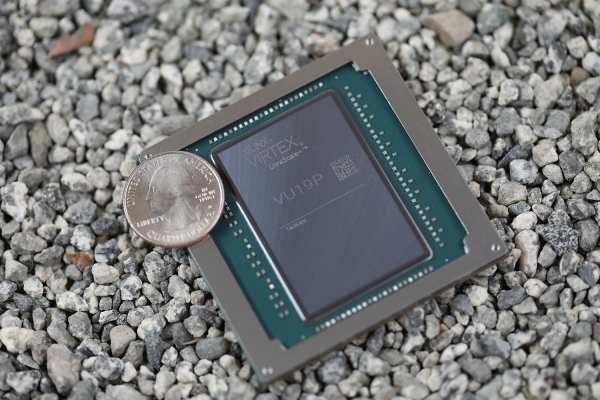
Xilinx announced on the 22nd that it is launching the 'Virtex UltraScale+ VU19P' FPGA.
With 35 billion transistors, the VU19P delivers high logic density and a large number of I/Os on a single device, enabling emulation and prototyping of future ASIC and SoC technologies, as well as test and measurement, computing, networking, aerospace, and defense applications.
The VU19P features up to 9 million system logic cells, up to 1.5 terabits per second of DDR4 memory bandwidth, up to 4.5 terabits per second of transceiver bandwidth, and over 2,000 user I/Os.
This enables prototyping and emulation of complex SoCs, as well as new complex applications used in AI, machine learning, video processing, and sensor fusion.It can develop complex algorithms. The VU19P is 1.6x larger than the 20nm Virtex UltraScale 440 FPGA, which was the industry's largest FPGA at the time of its launch.
“Developers can use the VU19P to accelerate hardware validation and begin software integration before deploying an ASIC or SoC,” said Sumit Shah, senior manager, product line marketing and management, Xilinx. “The VU19P comes with a robust, proven tool flow and IP to support this.”
The VU19P is supported by a comprehensive set of debug and visibility tools and IP, providing customers with a comprehensive development platform for rapidly designing and validating next-generation applications and technologies.
Through co-validation of hardware and software, developers can import software and implement custom features before actual components are delivered. Furthermore, by co-optimizing the design flow using the Vivado Design Suite, they can reduce costs and tape-out risks, accelerating time to market.
“Arm uses Xilinx devices as part of our verification process for our next-generation processor IP and SoC technology,” said Tran Nguyen, director of Design Services at Arm. “The VU19P will enable Arm and our many partners to accelerate the design, development and verification of our roadmap technologies.”
The VU19P is scheduled to be generally available in fall 2020.
Comments
Related news
Microchip Launches Low-Power FPGA Image Processing Solution
As vision-based systems that are computationally intensive become integrated at the network edge, FPGAs are positioning themselves as flexible platforms for next-generation designs. Microchip Technology, through its subsidiary Microsemi, has announced the Smart Embedded Vision Initiative to assist developers with rapid design by providing solutions for intelligent machine vision system design through Microchip's low-power PolarFire FPGAs. The Smart Embedded Vision Initiative offers an FPGA product family that includes IP, hardware, and tools for low-power, small form factor machine vision designs in industrial, medical, broadcast, automotive, aerospace, and defense markets.
2019.07.16by 이수민 기자
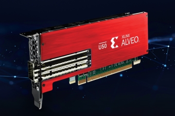
Xilinx Launches Adaptive Computing Accelerator 'Alveo U50'
Xilinx has launched the Alveo U50 data center accelerator card. The Alveo U50 is designed to handle critical workloads in computing, networking, and storage on a single reconfigurable platform, and is a low-profile adaptive accelerator card supporting PCIe Gen 4. The U50 can improve throughput, latency, and power efficiency by 10 to 20 times to address new dynamic workload challenges such as cloud microservices. By performing computing closer to data to accelerate networking and storage workloads, it enables developers to identify and eliminate latency and data movement bottlenecks.
2019.08.07by 이수민 기자

Xilinx Acquires Solarflare to Provide Integrated Platform Solutions
Xilinx changes data center market competition landscape with Solarflare acquisition. Through Solarflare's SmartNIC network interface card technology, capable of transmitting and receiving 100 million packets per second at under 75 watts.
2019.08.13by 명세환 기자

Intel Unveils Next-Generation 'Core Ultra Series 3' and vPro Platform for Enterprise PCs
Intel has officially unveiled the "Intel Core Ultra Series 3" for next-generation enterprise PCs and the latest vPro platform, addressing a wide range of demands from enterprise notebooks to high-performance workstations.
2026.03.26by 배종인 기자

ROHM Launches ESD Protection Diode Compatible with High-Speed Interfaces of 10Gbps or Higher
Semiconductor specialist ROHM has developed the 'RESDxVx series' of ESD (electrostatic discharge) protection diodes capable of responding to next-generation high-speed data communication environments exceeding 10Gbps, simultaneously enhancing both signal quality maintenance required in high-speed interfaces and IC protection performance.
2026.03.26by 배종인 기자











