


Four Consortia Launch Full-Scale Developing Domestic AI Semiconductors
 Published2020.04.24 12:11
서버·모바일·에지·공통 분야 NPU 10개 개발
올해부터 2029년까지 총 2,475억 투입 예정
AI 반도체 기술력 확보를 위해 과학기술정보통신부는 23일, 차세대 지능형 반도체 기술개발 사업의 2020년 신규과제 수행기관을 선정하고, 본격적인 기술개발에 착수한다고 밝혔다.
과기정통부와 산업통상자원부는 2020년부터 2029년까지 차세대 지능형 반도체 기술개발 사업에 1조96억 원을 투입하며, 그중 AI 반도체 설계 분야에만 2,475억 원을 투입한다.

2020년 신규과제는 분야별 기술 공유·연계와 연구성과의 결집을 위해 기존 개별과제 방식과는 다르게 각 세부과제를 통합하여 산학연 컨소시엄 형태로 개발하도록 기획됐다. 이에 따라 총 4개 컨소시엄, 28개 수행기관(기업 16곳, 대학 10곳, 출연연 2곳)이 선정됐다.
특히 SK텔레콤·텔레칩스·넥스트칩이 각각 서버·모바일·에지 분야 컨소시엄 총괄기관으로 참여하여 분야별 개발 결과물을 통합한 SoC 제작 및 실증 등의 역할을 할 예정이다.
과기정통부는 2020년에만 288억 원을 투입할 계획이다. 2020년 신규과제에서는 서버‧모바일‧에지·공통 분야에서 높은 연산성능과 전력효율을 갖는 다양한 AI 반도체, 즉 신경망 처리장치(Neural Processing Unit; NPU) 10개를 상용화 목표로 개발한다. 또한, 초고속 인터페이스, 소프트웨어까지 통합적인 개발로 AI 반도체 플랫폼 기술을 확보할 계획이다.
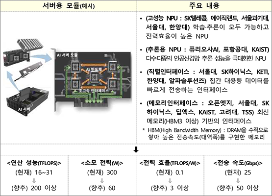

먼저 서버 분야에서는 SK텔레콤을 비롯한 15개 기관이 참여한 컨소시엄이 최대 8년간 총 708억 원을 투입하여 클라우드 데이터 센터 등 고성능 서버에 활용 가능한 NPU와 인터페이스를 개발한다.
컨소시엄은 향후 각 세부과제에서 개발된 NPU와 인터페이스를 통합하여 2PFLOPS(1초당 1조 번 부동 소수점 연산 처리 능력)급 이상의 성능을 갖는 서버(모듈)를 개발하고, 이를 SK텔레콤 클라우드 데이터 센터 등에 적용할 계획이다. 또한, 초고속 인터페이스 개발 결과물의 국제 표준화를 추진하고 SK하이닉스의 차세대 메모리 컨트롤러 등에 적용할 계획이다.
2단계 후속 과제(2025~2029)를 통해선 차세대 지능형 반도체 기술개발 사업 소자 분야에서 추진 중인 저전력 신소자 개발 결과물과 설계 기술을 융합하여 1PFLOPS급 NPU를 개발할 계획이다.
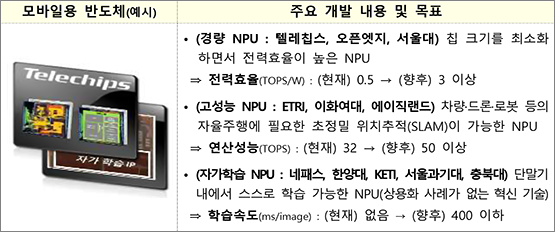
※ 1TOPS는 1초당 1조 번의 정수 연산 처리 능력을 의미
모바일 분야에서는 텔레칩스 등 11개 기관이 참여한 컨소시엄이 5년간 총 460억 원을 투입하여 자율주행차량, 드론 등 모바일 기기에 활용 가능한 NPU들을 개발한다.
컨소시엄은 향후 각 세부과제에서 개발된 NPU를 통합하여 텔레칩스의 차량용 반도체 제품 등에 적용할 계획이며, 이를 통해 ADAS 등 자율주행차량용 반도체 시장 등에 진출할 계획이다.
에지 분야에서는 넥스트칩 등 17개 기관이 참여한 컨소시엄이 5년간 총 419억 원을 투입하여 영상보안, 음향기기, 생체인증보안기기 등 IoT 디바이스에 활용 가능한 NPU들을 개발한다.
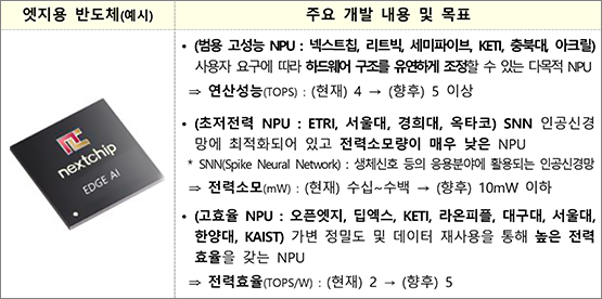
컨소시엄은 향후 개발된 결과물을 넥스트칩의 영상보안 장치(CCTV, 블랙박스 등)와 옥타코의 생체인증보안기기 등에 적용할 계획이다.
공통 분야에서는 ETRI와 카이스트가 5년간 총 52.6억 원을 투입하여 MRAM과 NPU를 통합하여 고효율 저전력(1mW급) PIM(Processing-In-Memory) 반도체 기술개발에 도전한다.
과기정통부와 산업부는 올 상반기 내 출범 예정인 범부처 사업단을 통해 과제별 성과관리, 사업화 등을 관리할 계획이며, 세계 시장 동향을 고려하여 조기 제품화가 가능하도록 유연한 목표관리를 추진할 계획이다.
매년 전문가가 참여하는 연차평가를 통해 세부과제별 성능 목표를 재점검하고, 충분한 시장 경쟁력을 갖는 제품이 개발될 수 있도록 목표 조정(Moving Target)을 해나갈 방침이다.
과기정통부 최기영 장관은 “이번 사업은 소자, 설계, 장비·공정 기술 등 산업부와 공동으로 준비한 예타 사업의 일환”이라며, “향후 기존 연구개발 성과를 민간에 확대하고, 차세대 PIM 기술 등 민간의 기술혁신을 뒷받침할 계획”이라고 밝혔다.
Comments
Related news

Arm Unveils Two IPs That Boost IoT Machine Learning Performance by 480x
Arm has unveiled the Cortex-M55 processor and Ethos-U55 microNPU, delivering on-device machine learning processing performance for small IoT and embedded devices. The Cortex-M55 achieves 15 times higher ML performance and 5 times higher DSP performance compared to the previous generation Cortex-M through Arm's Helium vector processing technology. Additionally, when paired with the Ethos-U55, ML performance can be improved by 480 times compared to existing Cortex-M processors.
2020.03.04by 이수민 기자
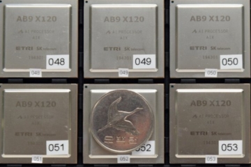
An AI semiconductor capable of 40 trillion calculations per second has been developed using domestic technology.
ETRI and SKT have successfully developed an AI semiconductor for the first time in Korea that can be utilized in high-performance servers. The developed chip integrates 16,384 cores in a coin-sized area, is capable of processing 40 trillion data operations per second, and consumes 15~40W of power. The developed chip will be demonstrated in SKT data centers starting in the second half of this year.
2020.04.08by 이수민 기자
Smart IoT sensors that “predict and judge” are the key to advanced manufacturing
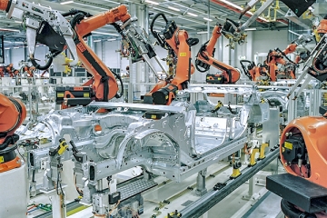
Smart factories can identify correlations between phenomena and issues occurring at production sites using smart sensors and resolve equipment failures and quality defects. If various sensors and devices are wirelessly integrated to autonomously gather information, and the production system evolves into an AI-based system that analyzes and leverages the collected information, enterprises can establish flexible production systems capable of responding in real time to changes in market conditions and customer demands.
2020.04.21by 이수민 기자
[e4ds Tech Day 2026 ⑨] Sim Sang-gyu, Autocrypt CTO: "In the Physical AI Era, Automotive Security Must Extend Beyond the Vehicle"
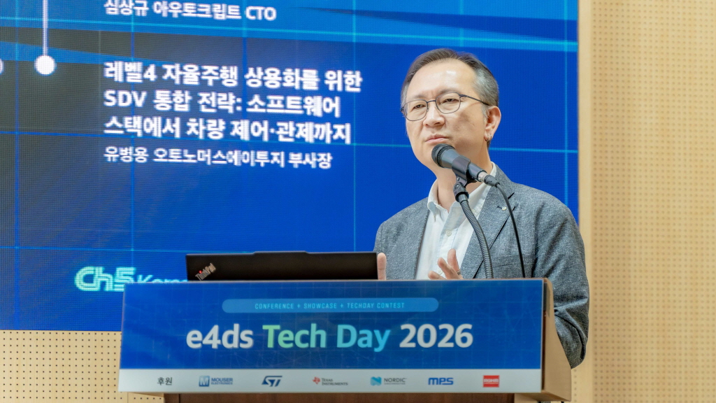
At e4ds Tech Day 2026, Sim Sang-gyu, CTO of Autocrypt, explained automotive cybersecurity strategies in the era of Physical AI and SDV (Software-Defined Vehicle). Automobiles are evolving as part of an ecosystem connected to AI, cloud, chargers, IoT, and robots, and he emphasized that the scope of security must expand beyond the vehicle interior to the entire connected environment. In particular, AI model tampering, adversarial attacks, OTA updates, and EV charger hacking were identified as major threats. He explained that response measures require zero trust, AI model integrity protection, intrusion detection, Security by Design and Default, and full lifecycle security management, and that proactive security system establishment beyond regulatory compliance is critical for securing future mobility competitiveness.
2026.10.12by 배종인 기자
NVIDIA to Invest $1 Billion in U.S. Science Over Next Five Years
NVIDIA has announced plans to invest $1 billion over the next five years to strengthen U.S. scientific and technological competitiveness. The company will enhance cutting-edge artificial intelligence research and development capabilities in key areas including quantum computing, healthcare, and energy security, while expanding support for higher education research institutions and cloud service providers. NVIDIA is participating as a major industry partner in the White House Office of Science and Technology Policy's Genesis Mission, and is promoting supercomputer construction in collaboration with national laboratories including Argonne and Los Alamos.
2026.10.12by 배종인 기자











