



Samsung Electronics to Build 5nm EUV Foundry Production Line in Pyeongtaek
 Published2020.05.21 11:01
Construction begins this month, with operations scheduled for the second half of 2021.
Samsung Electronics announced on the 21st that it will build a foundry production facility at its Pyeongtaek campus in Gyeonggi Province to respond to the growing demand for Extreme Ultra Violet (EUV)-based products.
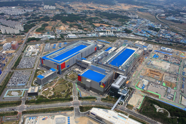
Following the launch of the EUV-dedicated "Hwaseong V1 Line" in February of this year, Samsung Electronics is expanding the scope of application of its ultra-fine process technology to various fields, including mobile, HPC (High Performance Computing), and AI, by establishing a foundry line in Pyeongtaek.
This investment is one of the follow-up measures to Samsung Electronics' "Semiconductor Vision 2030," announced in April of last year. Samsung Electronics began construction on its Pyeongtaek foundry line this month, with full operations planned for the second half of 2021.
Since Samsung Electronics began mass production of EUV-based 7nm process technology at the Hwaseong S3 Line in 2019, it has continued to expand its ultra-fine process production scale through the V1 Line in 2020. When the Pyeongtaek line comes online in 2021, production of products based on ultra-fine processes of 7 nanometers or less is expected to increase further.
Additionally, the company plans to mass-produce 5nm products first in Hwaseong in the second half of this year, followed by main production at the Pyeongtaek foundry line.
Meanwhile, the global foundry market is expected to see growth driven by ultra-fine processes, driven by the proliferation of new applications such as 5G, HPC, AI, and networking. Samsung Electronics plans to expand the application of advanced EUV processes to high-end mobile devices and new applications, starting with premium mobile chips.
Comments
Related news

Samsung Electronics Establishes Mass Production System for 1st Generation 10nm-Class EUV DRAM
Samsung Electronics has supplied one million units of its first-generation 10-nanometer-class DDR4 DRAM modules produced using EUV process technology to customers, presenting a new paradigm to overcome the limitations of semiconductor fine-process technology. The fourth-generation 10-nanometer-class DRAM manufactured using EUV has doubled productivity per 12-inch wafer compared to the first-generation 10-nanometer-class DRAM.
2020.03.25by 최인영 기자
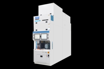
ACM Enters Semiconductor Dry Process Market with 'Ultra Furnace'
ACM Research has unveiled an Ultra Furnace for semiconductor dry process applications. The Ultra Furnace is optimized for low-pressure chemical vapor deposition processes. By changing only a few components and the layout, it can be applied to oxidation processes, thermal treatment processes, and atomic layer deposition processes as well.
2020.05.12by 이수민 기자
DB HiTek posts record quarterly results thanks to rising demand for power semiconductors.
DB Hightech recorded sales of 225.8 billion won and operating profit of 64.7 billion won in the first quarter of this year. This represents increases of 41% and 189%, respectively, compared to the same period last year, marking record highs for both sales and operating profit on a quarterly basis, with an operating profit margin of 29%.
2020.05.15by 이수민 기자

Intel Unveils Next-Generation 'Core Ultra Series 3' and vPro Platform for Enterprise PCs
Intel has officially unveiled the "Intel Core Ultra Series 3" for next-generation enterprise PCs and the latest vPro platform, addressing a wide range of demands from enterprise notebooks to high-performance workstations.
2026.03.26by 배종인 기자

ROHM Launches ESD Protection Diode Compatible with High-Speed Interfaces of 10Gbps or Higher
Semiconductor specialist ROHM has developed the 'RESDxVx series' of ESD (electrostatic discharge) protection diodes capable of responding to next-generation high-speed data communication environments exceeding 10Gbps, simultaneously enhancing both signal quality maintenance required in high-speed interfaces and IC protection performance.
2026.03.26by 배종인 기자











