



Samsung Electronics Supports Korean Fabless Companies with SAFE-CDP Chip Design Platform
 Published2020.06.19 08:31
Providing SAFE-CDP, a design platform, to small and medium-sized fabless companies.
Samsung Electronics announced on the 18th that it will provide a platform for designing semiconductor chips in the cloud to domestic small and medium-sized fabless companies to strengthen the competitiveness of the domestic system semiconductor ecosystem.
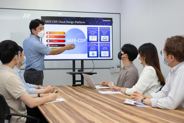
Receiving SAFE-CDP training [Photo = Samsung Electronics]
Last April, Samsung Electronics announced plans to strengthen its system semiconductor ecosystem. Since then, it has expanded its Multi-Project Wafer (MPW) program for domestic small and medium-sized fabless companies to operate three to four times per process annually. It also offers opportunities to utilize 8-inch (200mm) and 12-inch (300mm) wafer processes.
Since the second half of 2019, Samsung Electronics has been providing technical training, including layout, design methodology, and verification, to domestic fabless companies and design houses. A Samsung Electronics representative stated that products developed through collaborations with small and medium-sized companies following the announcement of its ecosystem strengthening plan are scheduled for mass production starting in late 2020.
◇ SAFE-CDP Supports Chip Design for Small and Medium-Sized Fabless Companies in the Cloud
Samsung Electronics has been operating the foundry ecosystem program 'SAFE (Samsung Advanced Foundry Ecosystem)' since 2018. Accordingly, we recently launched the ‘Integrated Cloud Design Platform (SAFE Cloud Design Platform; SAFE-CDP)’.
SAFE-CDP, jointly developed by Rescale and Samsung Electronics, is a service that provides a virtual design environment so that fabless customers can immediately begin chip design with just an idea.
This service is a platform built to enable the SW of automation design SW companies Ansys, Mentor (a Siemens Business), Cadence, and Synopsys to run on the public cloud.
As processes become more refined, semiconductor chip design becomes more complex and challenging. As the design process progresses, the computing resources required increase exponentially, and the time required for chip verification becomes significant.
SAFE-CDP reduces customers' investment burden for server expansion and allows them to flexibly use computing resources required for chip design and verification work according to stage.
A Samsung Electronics official stated that Gaonchips, a domestic fabless company, used SAFE-CDP to shorten the design time for automotive semiconductor chips by approximately 30% compared to previous models. The official added that several domestic companies, including AD Technology and Hanatech, have expressed interest in using SAFE-CDP.
Comments
Related news
Ten Korean fabless companies will be granted free access to Arm IP.
The Ministry of SMEs and Startups and Arm have concluded a comprehensive business agreement to support the growth of domestic semiconductor startups and venture companies. Under the agreement, Arm will provide Arm Flexible Access to the Ministry of SMEs and Startups for the next three years, while the Ministry will select ten startups and venture companies annually and provide support for them to utilize Arm's IP for one year.
2020.04.22by 이수민 기자
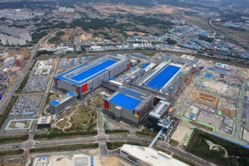
Samsung Electronics to Build 5nm EUV Foundry Production Line in Pyeongtaek
Samsung Electronics announced that it will establish a foundry production facility at its Pyeongtaek campus in Gyeonggi Province to respond to demand for EUV-based products. Samsung Electronics has commenced construction of the Pyeongtaek foundry line this month, with plans to begin full-scale mass production of 5-nanometer products from the second half of 2021.
2020.05.21by 이수민 기자
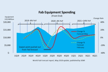
Signs of a surge in investment in memory, image, and power semiconductor equipment are emerging.
According to SEMI's World Fab Forecast report, semiconductor fab equipment investment in 2021 is projected to reach $67.7 billion, representing approximately 24% growth compared to 2020. Memory fabs are expected to make the largest investment at around $30 billion, followed by logic fabs and foundries at $29 billion.
2020.06.10by 강정규 기자

Intel Unveils Next-Generation 'Core Ultra Series 3' and vPro Platform for Enterprise PCs
Intel has officially unveiled the "Intel Core Ultra Series 3" for next-generation enterprise PCs and the latest vPro platform, addressing a wide range of demands from enterprise notebooks to high-performance workstations.
2026.03.26by 배종인 기자

ROHM Launches ESD Protection Diode Compatible with High-Speed Interfaces of 10Gbps or Higher
Semiconductor specialist ROHM has developed the 'RESDxVx series' of ESD (electrostatic discharge) protection diodes capable of responding to next-generation high-speed data communication environments exceeding 10Gbps, simultaneously enhancing both signal quality maintenance required in high-speed interfaces and IC protection performance.
2026.03.26by 배종인 기자











