



RF-to-bit development platform accelerating phased array system design
 Published2020.09.03 12:15
멀티채널 RF 시스템 제품 개발 과정 간소화
미래의 안테나 설계에는 위상 배열(Phased array)이 구현돼야 한다.
달라진 기술 동향과 빠른 시장 출시 압력은 위상 배열 시스템의 RF 설계자에게 ▲멀티채널 환경에서 RF 전자장치 확인 ▲채널 간 동기화 및 캘리브레이션 확인 ▲생산 하드웨어 개발과 병행한 소프트웨어 개발 등의 과제들을 안겨준다.
이러한 과제들을 해결할 수 있도록 ADI는 소프트웨어로 구성 가능한 고속 컨버터를 기반으로 하는 멀티채널 RF-to-bit 개발 플랫폼을 출시했다. 이 플랫폼은 데이터 컨버터, RF 분배, 전력 제어, 16채널 클럭 공급, 다이렉트 S-밴드 샘플링 솔루션을 포함한다.
통합 RF 샘플링 고속 컨버터
최근 출시된 고속 컨버터는 모놀리식 실리콘에 ADC, DAC 및 디지털 시그널 프로세싱 블록을 통합했다.
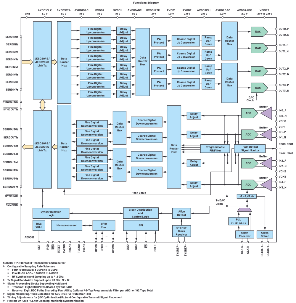
위의 그림에 보이는 MxFE™ 4채널 16비트 12 GSPS 성능의 RF DAC와 4채널 12비트 4 GSPS 성능의 RF ADC는 그 예로, 4개의 ADC와 4개의 DAC 및 디지털 업/다운 컨버터 뿐 아니라 NCO(Numerically controlled oscillator)와 FIR(Finite-impulse response) 디지털 필터를 포함하고 있다.
DAC는 12 GSPS 샘플링 속도로 정격 지정되고, ADC는 4 GSPS로 지정된다. 아날로그 대역폭은 S-밴드에서 낮은 C-밴드까지 직접 샘플링 및 파형 생성을 제공한다.
이 컨버터는 더 많은 RF 스펙트럼 대역을 처리하고, DSP 기능을 온칩 내장하고 있어 사용자는 특정 무선 신호 대역폭 요구사항을 만족하도록 프로그래밍 가능한 필터와 디지털 업/다운 컨버전 블록을 구성할 수 있다.
전용 실리콘에는 임베디드 프로세싱 기능이 내장돼 FPGA에서 이러한 기능을 수행하는 아키텍처보다 전력 소모를 크게 줄일 수 있다.
설계자는 자유롭게 이용할 수 있는 유용한 FPGA 자원을 확보할 수 있어 더 비용효율적인 FPGA를 사용하거나 FPGA의 여유 자원을 더 높은 수준의 시스템 애플리케이션 프로세싱에 할당할 수 있다.
16채널, 다이렉트 RF 샘플링 개발 플랫폼
아래의 사진은 16채널, 다이렉트 RF 샘플링 개발 플랫폼이다.
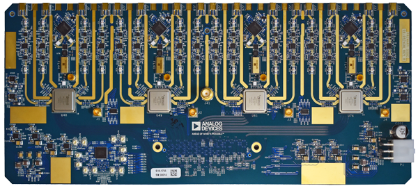

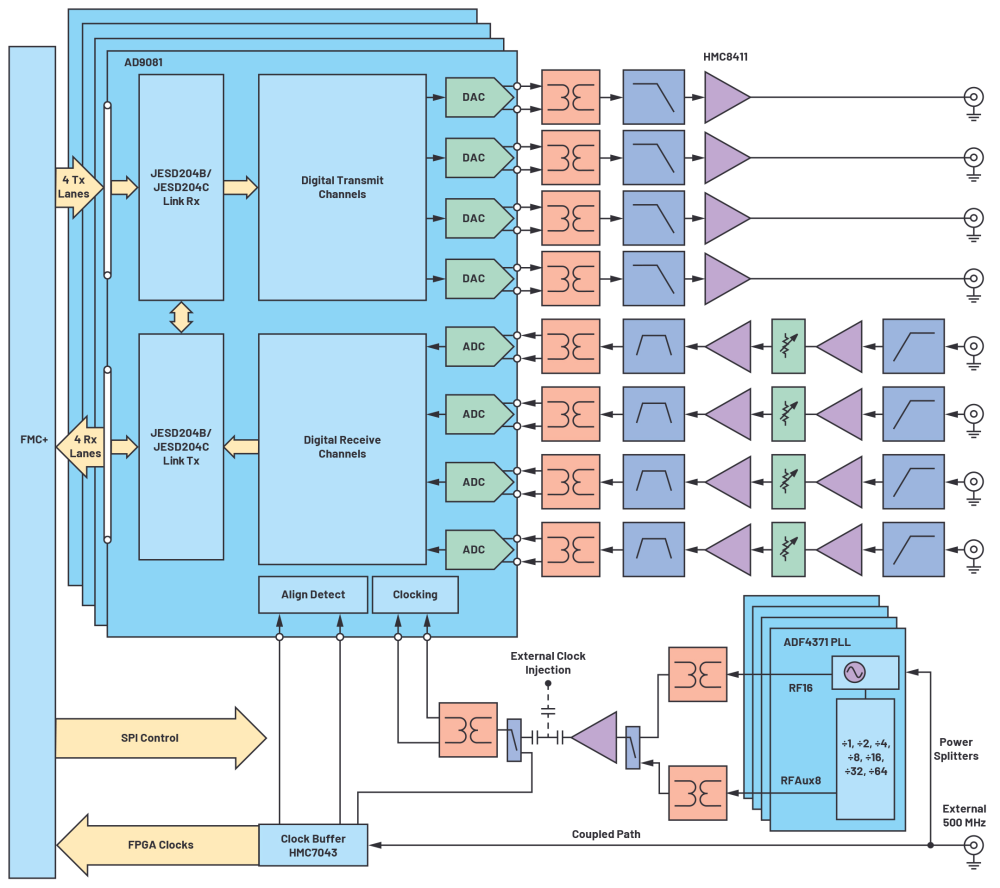
이 통합 컨버터는 혼성 신호 프런트엔드(MxFE)라고 부르며, 16채널 보드는 4개의 MxFE를 포함하므로 ‘쿼드 MxFE’라 이름 붙여졌다. 1개의 MxFE마다 각각 4개의 DAC와 ADC를 포함하므로 쿼드 MxFE에는 총 16개의 송신 채널과 16개의 수신 채널이 존재한다.
RF 부는 발룬, 증폭기, 필터를 포함하므로 RF 인터페이스를 간소화한다.
트랜시버 채널에는 DAC 이미지 억제를 위한 저역 통과 필터 및 DAC 출력에 이득 블럭이 함께 한다. 리시버 채널에는 2차 나이키스트 샘플링을 위한 대역 통과 필터와 함께 2개의 이득 단과 이득 제어가 포함된다.
필터는 미니서킷(Mini-Circuits)의 1206 필터 풋프린트에 들어가므로 사용자는 다른 애플리케이션을 위한 필터로 바꿀 수 있다.
채널 간격은 T/R 쌍당 600mils로 구현되며, X-밴드, 반(半)파장, 단극 요소 격자 간격을 지원한다. 이 풋프린트에서 이 제품은 최대 X-밴드 주파수까지 모든 요소의 디지털 빔포밍 시스템과 호환된다. 쿼드 MxFE가 S-밴드를 직접 생성하므로 별도의 RF 믹서 1개를 추가하면 X-밴드 주파수 동작을 실행할 수 있다.
클러킹 회로가 포함되어 있으며, 모든 클럭은 공통 레퍼런스 주파수에서 가져온다. PLL은 컨버터별로 제공되며, 레퍼런스 주파수에 위상 동기되고 AD9081 클럭 입력을 제공한다. 대체 컨버터 클럭 소스를 이용한 평가를 위해 테스트 포인트 삽입 옵션이 제공된다.
디지털 클럭 또한 공통 레퍼런스 주파수에서 유도된다. 클럭 칩이 포함돼 동기화를 위해 AD9081에 SYSREF를, FPGA를 위해 필요한 클럭을 제공할 뿐 아니라, 옵션으로 AD9081에 내부 PLL을 사용할 수 있게 하는 레퍼런스 주파수를 제공한다.
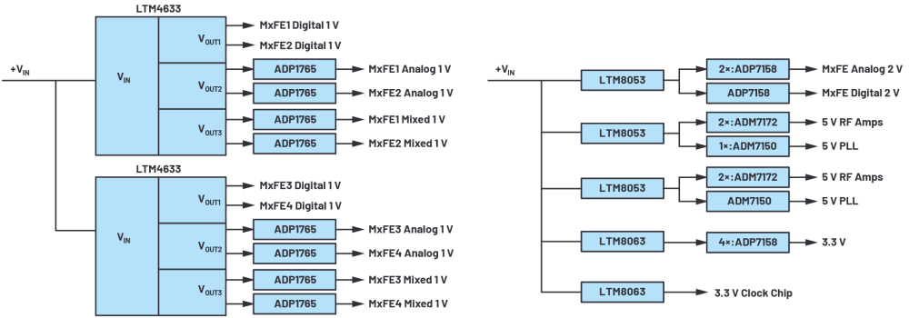
위의 그림을 보면 전력 분배와 레귤레이션이 포함된 것을 알 수 있다. 필요한 모든 전압은 단일 12V 입력에서 가져온다. 전력 분배 설계는 스위칭 레귤레이터 뒤쪽에, 예민한 아날로그 전압을 위한 저잡음 선형 레귤레이터가 결합하는 구조가 포함된다.
소프트웨어 제어
소프트웨어, 펌웨어 및 FPGA 코드는 플랫폼을 더 높은 수준의 프로세싱 언어로 제어할 수 있도록 개발되었다.
또한 모델을 개발하는 시스템 엔지니어가 MATLAB 환경에서 하드웨어에 직접 연결할 수 있도록 MATLAB 스크립트와 GUI가 작성되었다.
MATLAB 인터페이스는 시뮬레이션에서 시험된 맞춤형 파형을 하드웨어에서 직접 평가할 수 있게 한다. 수신 데이터 캡처 인터페이스를 활용하면 수신 데이터에 대한 특정 프로세싱이 가능하다.
소프트웨어와 펌웨어는 모두 오픈소스로서, 이 점은 최신 트랜시버 또는 컨버터를 기반으로 하는 다른 ADI 모듈 제품들과 유사한 특성이다.
쿼드 MxFE, RF 시스템 개발의 프로토타이핑 단계 제거
범용 프로토타이핑 환경을 구현하는 쿼드 MxFE RF-to-bit 개발 플랫폼은 설계자에 △전체 컨버터 IC 및 보드에서 멀티채널 동기화를 보여주는 개발 플랫폼 △멀티채널을 동시에 테스트하기 위한 목적으로 생산설계를 진행하기 전, 평가 보드 환경에서의 멀티채널 성능 검증을 제공한다.
또한, △하드웨어 생산과 소프트웨어 개발을 병행할 수 있게 하는 통합 및 기능 수준 △RF I/O, 클러킹 및 동기화 회로, 전력 분배, 고속 디지털 I/O 라우팅을 포함하여 고속 컨버터를 둘러싼 모든 회로의 레퍼런스 디자인 등을 지원한다.
이를 조합하면 멀티채널 RF 시스템 제품 개발에서 프로토타이핑 단계를 제거할 수 있어, RF 엔지니어는 시스템 솔루션에 보다 집중할 수 있다.
RF-to-bit 개발 플랫폼이 당초 설계된 목적은 위상 배열 개발을 위해서였다. 하지만 플랫폼이 제공하는 범용성 덕분에 레이더, EW, 5G 및 계측 애플리케이션과 같은 모든 멀티채널 RF 시스템에 적용할 수 있었다.
그 결과, 설계자들은 진정한 의미의 소프트웨어 정의 멀티채널 환경을 제공하는 단일 하드웨어, 다중 애플리케이션 플랫폼을 만날 수 있게 됐다.
이 기사는 아나로그디바이스의 피터 델로스(Peter Delos), 찰스 프릭(Charles Frick), 마이크 존스(Mike Jones) 엔지니어가 공저한 ‘신속한 프로토타이핑이 가능한 위상 배열용 멀티채널 RF-to-Bit 개발 플랫폼(Multichannel RF-to-Bits Development Platform Enables Rapid Prototyping for Phased Arrays)’이란 제목의 글을 정리한 것입니다.
Comments
Related news

ADI Unveils the ADRV9002, a Wide Dynamic Range RF Transceiver
ADI has launched the ADRV9002 RF transceiver, suitable for commercial and military applications. The ADRV9002 RF transceiver operates in the 30MHz to 6GHz frequency range and provides a receiver with a -150dBc/Hz dynamic range and a transmitter with high linearity.
2020.07.24by 명세환 기자
.png)
Mouser to Supply Panasonic BLE Modules for Remote Control Devices
Mouser Electronics supplies Panasonic's PAN1740A BLE RF module. The PAN1740A module features a fully integrated baseband processor and wireless transceiver for BLE 5.0 connectivity, supports up to 8 simultaneous connections, and reduces boot time. Additionally, it is optimized for remote control devices requiring gesture recognition and voice command support.
2020.08.27by 이수민 기자
ST Adds QFN48 Package Option to STM32WLE5 RF SoC
ST Microelectronics has added a QFN48 package option to its STM32WLE5 wireless SoC portfolio to support diverse industrial wireless applications. Based on STM32L4 ultra-low-power MCU technology, the STM32WLE5 integrates Semtech's SX126x sub-GHz wireless transceiver. Long-term availability is assured as ST's 10-year lifetime warranty for industrial products is supported.
2020.09.01by 강정규 기자

Intel Unveils Next-Generation 'Core Ultra Series 3' and vPro Platform for Enterprise PCs
Intel has officially unveiled the "Intel Core Ultra Series 3" for next-generation enterprise PCs and the latest vPro platform, addressing a wide range of demands from enterprise notebooks to high-performance workstations.
2026.03.26by 배종인 기자

ROHM Launches ESD Protection Diode Compatible with High-Speed Interfaces of 10Gbps or Higher
Semiconductor specialist ROHM has developed the 'RESDxVx series' of ESD (electrostatic discharge) protection diodes capable of responding to next-generation high-speed data communication environments exceeding 10Gbps, simultaneously enhancing both signal quality maintenance required in high-speed interfaces and IC protection performance.
2026.03.26by 배종인 기자











