



Korea Institute of Machinery and Materials (KIMM) is producing large, affordable transparent displays and semiconductors.
 Published2021.05.12 16:41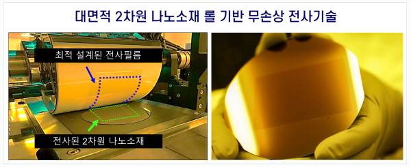
The technology to produce large-scale transparent displays and transparent semiconductors cheaply and quickly has been developed, and is expected to be used in various fields such as autonomous driving and displays.
The Korea Institute of Machinery and Materials (President Park Sang-jin), under the Ministry of Science and ICT, has developed a 'large-area 2D nanomaterial damage-free roll transfer technology' that can transfer 2D nanomaterials of atomic layer thickness to wafer size without damage.
It is expected that this breakthrough will accelerate the commercialization of the technology by significantly improving the nanomaterial transfer process, which can be utilized in various fields, including transparent displays, transparent semiconductors, and displays for autonomous vehicles.
Kim Gwang-seop, a senior researcher at the Nanomechanics Equipment Laboratory at the Korea Institute of Machinery and Materials, has developed a technology that can transfer two-dimensional nanomaterials less than 1 nm thick, which is about 1/50,000th the thickness of a human hair, onto a wafer substrate larger than 4 inches without damage.
Roll-based transfer processes transfer nanomaterials located on the surface of a transfer film onto a desired substrate. This highly efficient manufacturing technology enables the continuous transfer of nanomaterials over large areas, much like printing with a roller.
The transfer process is divided into a transfer film (A) with the nanomaterial to be transferred and a substrate (B) onto which the nanomaterial is transferred. Roll transfer involves rolling A over B, as if using a roller, and the material on A is transferred onto B. This process is similar to attaching a tattoo to the skin using a tattoo sticker. A sticker with a tattoo pattern attached can be likened to a transfer film, a tattoo pattern to a two-dimensional nanomaterial or micro-element, and skin to a target substrate.
The key to this technology is that it successfully eliminated instability, such as tearing when removing thin nanomaterials or breaking when attaching them to a substrate, when transferring two-dimensional nanomaterials.
The research team optimized the thickness of the adhesive layer of the transfer film to eliminate instability at the peeling surface. They discovered a principle that allows even the thinnest and most delicate tattoo stickers to be transferred intact without damage when peeling them from the film and applying them to the skin.
The research team observed two different types of damage occurring in the transfer film depending on the adhesive layer thickness. Based on this, they used computational simulations and experiments to elucidate the damage mechanism of the two-dimensional nanomaterial due to adhesive layer deformation and optimized the adhesive layer thickness.
It is expected that the results of this research will reduce nanomaterial damage occurring during the roll transfer process of two-dimensional nanomaterials from approximately 30% to 1%.
Kim Gwang-seop, a senior researcher at the Korea Institute of Machinery and Materials, said, “These research results will be able to drastically reduce the manufacturing cost of wearable electronic devices, flexible transparent displays, and high-performance bio/energy sensors based on two-dimensional nanomaterials and microdevices.” He added, “We also expect that it will be possible to create new industries utilizing two-dimensional nanomaterial-based flexible transparent electronic devices in various fields such as next-generation semiconductors, displays, and future automobile industries.”
Meanwhile, this research was conducted with support from the Ministry of Science and ICT's basic project for machinery and equipment, 'Development of core technology for flexible transparent display nano-based production equipment for autonomous vehicles', and the government's Ministry of Science and ICT's global frontier project, 'Development of micro-LED-based meta-display technology'.

Comments
Related news
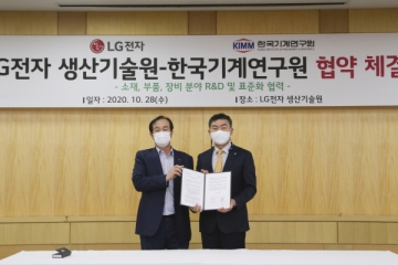
Korea Machinery & Materials Institute-LG Production Technology Institute, Join Hands to Strengthen Manufacturing Equipment Technology Competitiveness
The Korea Institute of Machinery and Materials (hereinafter KIMM) and LG Electronics Production Technology Institute (hereinafter LG Production Technology Institute) have joined hands to advance equipment technology. KIMM signed an MOU for "cooperation in core technology development for materials, components, and equipment" with the LG Production Technology Institute, with Director Hong Soon-guk of the LG Production Technology Institute and other relevant personnel in attendance. The signing ceremony served as a venue for substantive exchange, including a review of research cooperation fields and discussion of specific future cooperation plans. Prior to this, KIMM and the LG Production Technology Institute held a technology exchange meeting in June and began identifying cooperative technologies.
2020.11.03by 강정규 기자
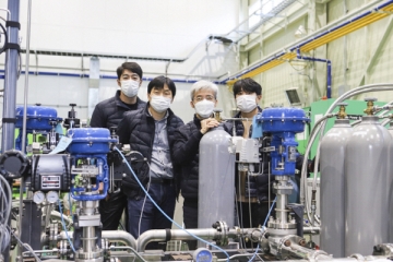
Korea Mechanical Engineering & Construction Co. develops Korea's first 'Neon' Brayton refrigeration system
The Korea Institute of Machinery and Materials (KIMM) has successfully developed Korea's first Brayton cryogenic refrigeration system using neon gas as the working fluid and demonstrated 2kW output at ultra-low temperatures of minus 200°C. With this successful development and demonstration of the ultra-low temperature refrigeration system, a foundation has been established for the localization of ultra-low temperature refrigeration systems, which currently rely entirely on foreign imports.
2020.12.18by 강정규 기자
Korea Institute of Machinery and Materials (KIMM) played a role in overcoming the mid-term COVID-19 crisis.
The Korea Institute of Machinery and Materials (KIMM, President Park Sang-jin) is implementing various customized programs including the 'KIMM SME-Tailored Problem-Solving Technology Support Project' and 'ACE Project' to assist small and medium-sized enterprises facing difficulties in technology development due to COVID-19.
2021.04.27by 배종인 기자

Intel Unveils Next-Generation 'Core Ultra Series 3' and vPro Platform for Enterprise PCs
Intel has officially unveiled the "Intel Core Ultra Series 3" for next-generation enterprise PCs and the latest vPro platform, addressing a wide range of demands from enterprise notebooks to high-performance workstations.
2026.03.26by 배종인 기자

ROHM Launches ESD Protection Diode Compatible with High-Speed Interfaces of 10Gbps or Higher
Semiconductor specialist ROHM has developed the 'RESDxVx series' of ESD (electrostatic discharge) protection diodes capable of responding to next-generation high-speed data communication environments exceeding 10Gbps, simultaneously enhancing both signal quality maintenance required in high-speed interfaces and IC protection performance.
2026.03.26by 배종인 기자











