


Samsung Electronics to Invest KRW 171 Trillion in System Semiconductors
 Published2021.05.14 08:57
Completion of Pyeongtaek Line 3 in the second half of 2022
Samsung Electronics is significantly expanding its investment to achieve its 'System Semiconductor Vision 2030'.
Samsung Electronics announced its additional investment plan for the system semiconductor sector through 2030 at the 'K-Semiconductor Belt Strategy Report Conference' held at its Pyeongtaek campus on the 13th.
To secure leadership in system semiconductors at an early stage, an additional 38 trillion won will be added to the 133 trillion won investment plan established at the time of the announcement of "System Semiconductor Vision 2030," for a total investment of 171 trillion won by 2030, and research and development of advanced foundry processes and construction of production lines will be further accelerated.
In April 2019, the government held a "System Semiconductor Vision Declaration Ceremony" at Samsung Electronics' Hwaseong plant and announced its plan to transform Korea into a comprehensive semiconductor powerhouse by fostering system semiconductors. At this time, Samsung Electronics presented its 'System Semiconductor Vision 2030' and announced a 133 trillion won investment plan.
Over the past two years since the vision declaration ceremony, cooperation has been actively promoted among key members of Korea's semiconductor ecosystem, including semiconductor manufacturing companies including Samsung Electronics, fabless companies, material, component, and equipment companies at the core of the supply chain, and academia responsible for fostering excellent talent, and the foundation for achieving the vision has been steadily laid.
With an unprecedented semiconductor shortage occurring across all industries and governments around the world competing to secure a semiconductor supply chain, a key component of future industries, Samsung Electronics' expanded investment in system semiconductors is expected to further elevate the status of "K-semiconductors."
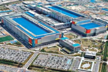
The cleanroom of Pyeongtaek Line 3, scheduled for completion in the second half of 2022, will be the size of 25 soccer fields. Featuring cutting-edge technologies, the fab will mass-produce 14nm DRAM and 5nm logic products using EUV technology. All processes are fully automated and managed by a smart control system.
As the world's largest semiconductor cluster, the Pyeongtaek campus is expected to further strengthen its leading role as a forward base for mass-producing cutting-edge products and a global semiconductor supply base.
Samsung Electronics plans to strengthen its position as the "world's No. 1" by proactively applying EUV technology to next-generation DRAMs, accelerating the development of future memory solution technologies such as "HBM-PIM," which combines memory and system semiconductors, and "CXL DRAM," which can overcome the capacity limitations of DRAM.
At the event, Samsung Electronics Vice Chairman Kim Ki-nam stated, “Even in the memory sector, where Korea has consistently maintained a leading position, the pursuit is fierce,” and added, “Rather than focusing on maintaining our lead, Samsung will take the lead in preemptive investment to widen the ‘super gap’ that can never be caught up to.”

Comments
Related news
.jpg)
Samsung Electronics' first-quarter sales reached KRW 65.3885 trillion, the highest quarterly figure ever.
Samsung Electronics achieved record operating profits for the first quarter based on strong set product sales including smartphones and increased OLED utilization rates.
2021.04.29by 배종인 기자
Is it possible for Samsung Electronics, with a market cap of 120 trillion won, to acquire NXP for 70 trillion won?
Articles are pouring out speculating on the possibility of Samsung Electronics acquiring NXP Semiconductors. This is because NXP has previously attempted to sell itself, and Samsung Electronics has declared its intention to pursue meaningful mergers and acquisitions within three years. However, the likelihood is not high because the profitability of the automotive semiconductor business is smaller than expected.
2021.04.29by 이수민 기자
510 trillion won investment in K-semiconductors by 2030
The government will complete the world's largest and most cutting-edge semiconductor supply chain through overwhelming private sector investment of over 510 trillion won by 2030 to realize comprehensive semiconductor superpower status.
2021.05.14by 배종인 기자

Intel Unveils Next-Generation 'Core Ultra Series 3' and vPro Platform for Enterprise PCs
Intel has officially unveiled the "Intel Core Ultra Series 3" for next-generation enterprise PCs and the latest vPro platform, addressing a wide range of demands from enterprise notebooks to high-performance workstations.
2026.03.26by 배종인 기자

ROHM Launches ESD Protection Diode Compatible with High-Speed Interfaces of 10Gbps or Higher
Semiconductor specialist ROHM has developed the 'RESDxVx series' of ESD (electrostatic discharge) protection diodes capable of responding to next-generation high-speed data communication environments exceeding 10Gbps, simultaneously enhancing both signal quality maintenance required in high-speed interfaces and IC protection performance.
2026.03.26by 배종인 기자











