



UNIST Develops Thin, Low-Power Quantum Dot TVs at Low Cost
 Published2021.06.04 15:51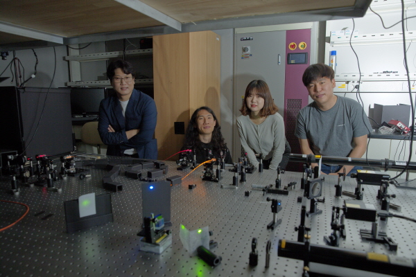
▲UNIST researchers who led this research (from left) Professor Park Kyung-deok, Researcher Lee Hyeong-woo, Researcher Koo Yeon-jeong, and Researcher Choi Jin-seong
Ultra-high brightness display application capable of brightness 100,000 times or more
A technology has been developed that can control the brightness and wavelength of quantum dot light by applying high pressure with an ultra-fine tip, raising expectations that it will be applicable to optical property analysis and display development.
A joint research team led by Professor Kyung-Deok Park of the Department of Physics at UNIST and Professor So-Hee Jeong of the Department of Energy Science at Sungkyunkwan University has succeeded in freely controlling the brightness and wavelength of light emitted by a single perovskite quantum dot particle.
The researchers used a technology that applies high pressure to perovskite quantum dots using the probe of an "active probe-enhanced photoluminescence nanomicroscope," inducing structural deformation and thereby altering the brightness and wavelength of quantum dot light. Notably, this technology can enhance the brightness of quantum dots by over 100,000 times, making it suitable for use in ultra-high-brightness displays.
Quantum dots are semiconductor particles that are just a few nanometers (nm) in size. It can emit light of a specific color on its own, making it possible to create thin and light TV or mobile phone screens that do not require backlights or color filters to emit light.
On the other hand, once quantum dots are synthesized, it is very difficult to control their luminescence characteristics, such as brightness and color, which has limited the development of application devices.
The research team was able to control the luminescence characteristics by applying pressure to perovskite quantum dots by connecting the atomic force probe of the 'active probe-enhanced photoluminescence nanomicroscope' to a piezoelectric element.
The 'active probe-enhanced photoluminescence nanomicroscope' is a technology previously developed by the research team. Because the controllable cross-sectional area is narrow at around 10 nanometers, the pressure (force applied to a unit area) can be increased to the gigapascal (GPa) level.
Another advantage of this technology is that mechanical strain in the quantum dot can be recovered when the probe is removed from the quantum dot.
Therefore, it is possible to prevent the problem of quantum dots being structurally damaged and resulting in reduced efficiency.
“Not only did we prove for the first time in the world that the properties of a single quantum dot can be reversibly controlled, but we also presented a solution to the problem of reduced efficiency, which was a limitation of existing quantum dot luminescence energy control research,” said Lee Hyeong-woo, a graduate student in the Department of Physics at UNIST who led the research. “This is a new study that breaks the conventional wisdom of existing quantum dot optical property control research.”
Using an 'active probe-enhanced photoluminescence nanoscopy', the research team was able to apply mechanical pressure while simultaneously analyzing the luminescence properties of quantum dots that change according to mechanical deformation with a spatial resolution of approximately 15 nanometers, which far exceeds the diffraction limit of light.
In particular, when quantum dots are placed between a gold-based atomic force probe and a gold thin film, it was confirmed that the luminescence intensity increases by about 100,000 times or more through the Purcell effect. Additionally, the energy band gap, which determines the color (wavelength) of the quantum dot, could also be changed.
Professor Park explained the significance of this research, saying, “If the wavelength-tunable, ultra-bright single perovskite quantum dot technology we presented this time is applied to next-generation displays, it will be possible to produce very thin, low-power quantum dot TVs at a much lower cost than now.” He added, “In addition to displays, it can also be used to develop various ultra-small nano-optoelectronic devices.”
Meanwhile, the 10-nanometer-sized perovskite quantum dots used in this study were produced by Professor Sohee Jeong's team at Sungkyunkwan University and Dr. Woo Joo-young at the Korea Institute of Industrial Technology, and Professor Moon-seok Jeong's team at Hanyang University's Department of Physics participated in the room-temperature stabilization process and basic characteristic analysis of the quantum dots.
Additionally, the theoretical calculations for the physical interpretation of the research results were led by Professor Yong-Hyeon Kim's team from the Department of Physics at KAIST.
The research results were published in the international journal ACS Nano on May 25th, and the core technology for controlling single quantum dot properties has been filed for domestic and European patents (PCT). The research was supported by the National Research Foundation of Korea, UNIST, and the Korea Institute of Industrial Technology.
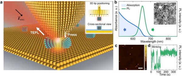
▲Illustration depicting strain control of perovskite quantum dots using a probe-enhanced photoluminescence nanoscopy.

Comments
Related news
UNIST Discovers Material to Lower Electric Vehicle Prices
Novel design principles for 'disordered rock salt materials,' which are attracting attention as next-generation electric vehicle battery materials, have been newly presented, providing momentum for the development of materials that can lower electric vehicle prices.
2021.05.10by 배종인 기자

Inorganic-based semiconductors to rise "also cheaper"
Adhesive health monitoring devices and foldable and rollable displays require flexible semiconductors. Most flexible semiconductors are organic-based, but a research team at UNIST's School of Advanced Materials Engineering has developed an inorganic-based flexible semiconductor. Since it can withstand high-temperature, high-pressure processes and exhibits good durability, it is expected to be applicable to the development of various flexible devices.
2021.05.17by 이수민 기자
Korea Institute of Machinery and Materials (KIMM) develops metamaterials, increasing infrared spectroscopy detection signal by 100 times.
Researchers from the Korea Institute of Machinery and Materials (KIMM, Director Park Sang-jin) under the Ministry of Science and ICT and UNIST (President Lee Yong-hoon) have developed a metamaterial that can dramatically improve processes for detecting hazardous substances and biomolecules.
2021.06.01by 배종인 기자

Intel Unveils Next-Generation 'Core Ultra Series 3' and vPro Platform for Enterprise PCs
Intel has officially unveiled the "Intel Core Ultra Series 3" for next-generation enterprise PCs and the latest vPro platform, addressing a wide range of demands from enterprise notebooks to high-performance workstations.
2026.03.26by 배종인 기자

ROHM Launches ESD Protection Diode Compatible with High-Speed Interfaces of 10Gbps or Higher
Semiconductor specialist ROHM has developed the 'RESDxVx series' of ESD (electrostatic discharge) protection diodes capable of responding to next-generation high-speed data communication environments exceeding 10Gbps, simultaneously enhancing both signal quality maintenance required in high-speed interfaces and IC protection performance.
2026.03.26by 배종인 기자











