


K-Semiconductor to launch large-scale feasibility studies in 2022
 Published2021.06.11 08:19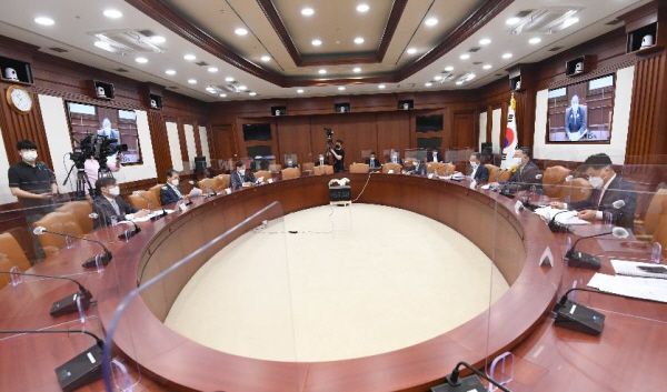
Advanced sensors and human resource development to be fully implemented in 2022.
A large-scale preliminary project to strengthen the semiconductor growth foundation, including the establishment of a K-semiconductor belt, the establishment of a small and medium-sized packaging base, large-scale human resource development, and the development of new technologies, will begin in earnest in 2022.
The government held the 11th Innovation Growth Big 3 (BIG3) Promotion Meeting on the 10th and announced the ‘K-Semiconductor Large-Scale Pre-Feedback Project Full-Scale Promotion Plan’ as a follow-up measure to the ‘K-Semiconductor Strategy’ jointly announced by relevant ministries on May 13th.
In this plan, the government has specified the key contents and future implementation plans of the five large-scale preliminary feasibility studies projects announced in the "K-Semiconductor Strategy," and plans to launch two of these projects in earnest starting in 2022.
First, starting in 2022, we will actively strengthen our technological capabilities in new fields such as advanced sensors and artificial intelligence to achieve new growth in the semiconductor industry.
Regarding the development of market-leading K-Sensor technology, the Ministry of Trade, Industry and Energy plans to support sensor technology development, while local governments plan to secure sensor manufacturing innovation platforms and verification infrastructure. They also plan to expedite related procedures to promote the "Market-Leading K-Sensor Technology Development" project starting in 2022.
PIM (Processing in memory) semiconductor technology that integrates memory and processor To lead, the Ministry of Trade, Industry and Energy and the Ministry of Science and ICT support the acquisition of capabilities in four major technological fields.
The 'PIM Artificial Intelligence Semiconductor Technology Development' project is scheduled to begin in earnest in 2022 after consultation with the budget authorities following the conclusion of the preliminary feasibility study.
To establish the K-semiconductor belt, infrastructure development projects such as a small and medium-sized business mass production test bed and an advanced packaging platform, as well as large-scale human resource development projects, which are key to the semiconductor growth foundation, will be implemented starting in 2023 after additional business planning.
A mass production test bed is planned to be built within the Yongin Semiconductor Cluster, and a semiconductor small and medium-sized business solidarity and cooperation ecosystem will be fostered through mass production-level clean rooms and early verification of performance and effectiveness linked to mass production fabs. The mass-produced test beta project is scheduled to apply for a preliminary feasibility study in the second half of this year.
To strengthen advanced packaging capabilities that enable high-performance, multi-functional, and miniaturized semiconductors, we will establish an infrastructure that provides one-stop support for prototype manufacturing, testing, evaluation, and certification.
The same platform will house approximately 90 pieces of equipment to apply and evaluate five cutting-edge packaging technologies, and will support domestic companies in the production and verification of prototypes and the implementation of technology development projects.
The advanced packaging platform business is planning to apply for a preliminary feasibility study in the second half of this year after supplementing the content.
To strengthen human resource development, which is key to revitalizing the semiconductor industry ecosystem, this project differs from existing projects in that companies and the government participate as joint investors with equal stakes, universities and research institutes carry out technology development projects based on companies' technological needs, and in the process, master's and doctoral level personnel acquire practical skills.
This project was ultimately rejected in the preliminary feasibility study conducted in the third quarter of 2020. However, considering the importance of semiconductor talent development and the current labor shortage within companies, the company plans to reapply for the preliminary feasibility study in the third quarter of 2021, and expand the project scale from the existing KRW 300 billion to KRW 350 billion.
Vice Minister of Trade, Industry and Energy Park Jin-gyu said, “Whether the public and businesses can actually feel the results of the ‘K-Semiconductor Strategy’ announced on May 13th depends on how faithfully the government implements follow-up measures.” He added, “Based on the active cooperation of various related ministries, we will smoothly implement follow-up tasks to realize a comprehensive semiconductor powerhouse, such as tax deductions, budget securing, financial support, and institutional improvement. We will continuously monitor the implementation status and additional support tasks through the Innovation Growth Big 3 (BIG3) Promotion Meeting and the Semiconductor Solidarity and Cooperation Committee.”

Comments
Related news
510 trillion won investment in K-semiconductors by 2030
The government will complete the world's largest and most cutting-edge semiconductor supply chain through overwhelming private sector investment of over 510 trillion won by 2030 to realize comprehensive semiconductor superpower status.
2021.05.14by 배종인 기자
Samsung Electronics to Invest KRW 171 Trillion in System Semiconductors
Samsung Electronics will invest a total of 171 trillion won by 2030, adding 38 trillion won to the original 133 trillion won investment plan established when announcing its 'System Semiconductor Vision 2030' to secure system semiconductor leadership early. The company will further accelerate research and development of advanced foundry processes and construction of production lines.
2021.05.14by 배종인 기자
Semiconductor Industry “Actively Welcomes K-Semiconductor Strategy”
The semiconductor industry has expressed its active support for the government's announced 'K-Semiconductor Strategy,' stating that it will accelerate corporate investment through tax incentives, financial support, and infrastructure assistance.
2021.05.14by 배종인 기자

Intel Unveils Next-Generation 'Core Ultra Series 3' and vPro Platform for Enterprise PCs
Intel has officially unveiled the "Intel Core Ultra Series 3" for next-generation enterprise PCs and the latest vPro platform, addressing a wide range of demands from enterprise notebooks to high-performance workstations.
2026.03.26by 배종인 기자

ROHM Launches ESD Protection Diode Compatible with High-Speed Interfaces of 10Gbps or Higher
Semiconductor specialist ROHM has developed the 'RESDxVx series' of ESD (electrostatic discharge) protection diodes capable of responding to next-generation high-speed data communication environments exceeding 10Gbps, simultaneously enhancing both signal quality maintenance required in high-speed interfaces and IC protection performance.
2026.03.26by 배종인 기자











