



[Interview] LPKF Korea CEO Lee Yong-sang: "We will provide laser solutions for processing a wider range of new materials."
 Published2021.08.06 13:57
까다로운 PCB 프로토타이핑 비용 및 시간 절감
첨단 DP, 통신 제품용 유리 가공 장비도 제공
산업계를 둘러싼 이슈들에 다양한 소재를 기반으로 하는 제품이 제작되고 있다.
일본 경제산업성은 2019년 7월, 반도체, 디스플레이 공정 관련 소재의 대한(對韓) 수출 규제를 시행했다. 국내 경제를 견인하는 핵심 수출 제품의 제조가 원천 차단될 수 있다는 우려는 업체의 소재 공급처 다변화와 국산 소재 개발로 이어졌다.
과학기술정보통신부는 올해 7월, 소재·부품·장비 R&D 지원 정책 본격화 2주년을 맞아 성과보고회를 개최하고, 2년 동안 9,241억 원이 투입돼 SCI급 논문 2,171건, 특허출원 1,570건, 특허등록 466건 등의 기술적 성과를 냈다고 밝혔다.
2020년 초엽 시작된 코로나19 팬데믹 사태는 전자제품 수요 상승을 이끌었고, 테슬라의 급속한 주가 상승과 이상 기후에 따른 탄소 배출 저감 기조는 자동차 업계의 전자화로 이어졌다. 새로운 소재와 부품, 장비가 속속 개발되는 가운데 제조업에선 이들을 활용한 고성능, 고정밀, 초소형 제품을 만드는 데 고심하고 있다.

본지는 LPKF 레이저 & 일렉트로닉스 코리아의 이용상 대표이사를 만나 레이저 가공과 관련한 제조업 동향, 인하우스 PCB 프로토타이핑 장비의 장점과 활용처, 그리고 유리와 신소재에 대한 가공 추세와 전망에 관해 묻는 시간을 가졌다.
Q. LPKF 레이저 & 일렉트로닉스 코리아는 어떤 기업입니까?
A. LPKF는 독일 증시에 상장된 레이저 관련 하이테크 기업입니다. LPKF 코리아는 독일 LPKF 본사의 100% 외국인 투자법인 공식 한국지사입니다.
지난 2014년 창립됐고, 2019년부터 한국 사업을 강화하기 위해서 대대적으로 조직을 개편해 현재에 이르고 있습니다. 현재는 3명의 경험 많은 세일즈 매니저와 2명의 전문 기술지원 및 애플리케이션 엔지니어가 주축을 이루고 있습니다.
Q. 레이저 가공 업계에서 LPKF 레이저 & 일렉트로닉스만의 차별점은?
A. LPKF는 1976년 설립돼 레이저를 이용한 다양한 소재의 가공이란 분야에만 집중해온 회사로서, 이에 대한 깊은 노하우를 축적하고 있습니다. 또한, 기존 레이저 소스 회사의 제품을 사용하기도 하지만, 레이저 소스를 개발하고 생산하는 자회사를 가지고 있어서 제품개발과 사후지원에도 많은 이점을 가지고 있습니다.
Q. 대표님께서 바라보시는 최근 제조 산업의 이슈는 무엇입니까?
A. 역사적으로 새로운 기술의 도약에는 그에 걸맞은 새로운 소재의 사용이 필수적이었습니다. 현재 많은 전자제품이 경박단소(輕薄短小) 트렌드를 따르고 있으며, 기존에 기계 부품의 비중이 월등히 높았던 자동차 산업도 빠르게 전자화되는 추세입니다. 휴대폰도 접히는 제품이 개발 중이며, 디스플레이도 이런 경향을 따를 것으로 보입니다. 이로 인해 커버 유리의 변화가 요구되고 있습니다.
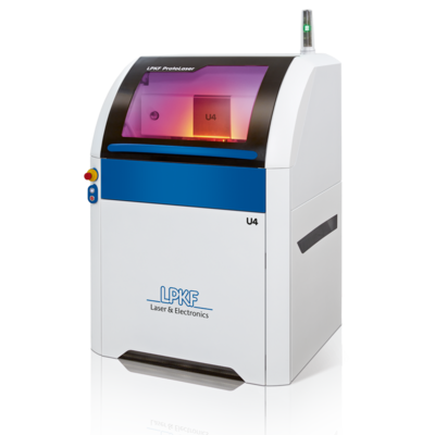

제품의 크기가 작아지면서 PCB 형상도 공간을 최대한 활용하기 위하여 복잡한 형태를 띠게 됐고, 두께는 얇아지고 있습니다. 이러한 PCB의 절단은 기존의 기계적인 라우터로는 한계가 있습니다. 차량의 전자화는 많은 변화를 요구합니다. 특히, 자율주행이 필수요소가 됨에 따라 부품들의 신뢰도를 놓이기 위한 노력이 수반되고 있습니다. 레이저 플라스틱 용접의 필요성이 점차 높아지는 이유입니다.
저는 LPKF 코리아가 이런 시장 변화에 충분히 대응할 수 있다고 믿고 있습니다.
Q. ‘나노 코리아 2021’ 행사에서 ‘프로토레이저(ProtoLaser)’ 등 PCB 프로토타이핑용 장비 등을 선보이셨는데, 이들 장비의 강점은 무엇입니까?
A. PCB 프로토타이핑이라는 분야가 생소할 수 있습니다. 현재는 개발단계에서도 대부분 외주를 통해 PCB를 제작합니다만, 이는 개발에 들어가는 비용과 시간을 늘립니다. 하지만, LPKF PCB 프로토타이핑 장비를 활용하면 연구실에서 몇 시간 만에 3D 툴로 제작한 회로를 만들고 테스트할 수 있어 비용과 시간을 줄일 수 있습니다. 특히 방산업체같이 비밀유지가 중요한 곳에서 수요가 많습니다.
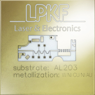
고정밀 성형이 가능하다 [사진=LPKF]
LPKF PCB 프로토타이핑 장비들은 5G, 6G 등 차세대 통신 관련 소재와 PCB 개발에도 사용되고 있습니다. 차세대 통신 제품은 기존 3G, LTE 제품보다 높은 정밀도와 미세선폭을 요구합니다. 해당 제품의 R&D 과정에서 LPKF 프로토레이저 같은 인하우스(in-house) 장비를 사용하면 비용과 시간을 절약할 수 있습니다.
저는 저희의 PCB 프로토타이핑 장비들의 활용처를 한정 짓지 않습니다. 프로토레이저 등의 장비는 소재 가공 장비라고 부를 수 있습니다.
최근 신소재 기반의 PCB를 요구하는 분야들이 많아지고 있습니다. 로봇이나 의료기기 분야가 대표적입니다. 실제로 기존 PCB 소재가 아닌 전혀 새로운 소재를 기반으로 하는 제품을 제작하는 데 저희 장비들이 사용되고 있습니다.
국내 의료기기 스타트업인 ‘토닥(TODOC)’은 인공와우 개발에 저희 제품을 활용하여 기존 제품을 월등히 뛰어넘는 혁신 제품을 만들었습니다.
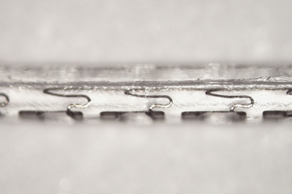
현재 KFDA 인증을 받는 중이며, 조만간 완전 상용화가 가능할 것으로 보입니다. 이런 장비는 전형적인 기술주도 국가에서 수요가 높습니다. 주요 구매국가로는 미국, 중국, 일본, 유럽 국가들이 있습니다. 국내 도입 가능성도 크다고 봅니다.
Q. 최근 무선 충전이나 유연한 디스플레이 등을 강점으로 내세우는 제품들이 늘면서 유리 가공 솔루션에 대한 전자 업계의 관심이 높을 것 같습니다.
A. 제조 업계에서 유리는 최근 가장 주목받는 소재라고 할 수 있습니다. 다양한 형태의 디스플레이가 나오고 있으며, 앞으로도 나올 것으로 예상됩니다.
LPKF는 유리 가공 분야에 LIDE(Laser Induced Deep Etching) 이라는 특허 기술을 가지고 있습니다. 이 기술로 기존 에칭 방식이나 레이저 직접 가공 방식의 미세균열 및 편평도(aspect ratio) 문제를 해결했습니다. 또한, 대량생산에 적합하고, 비용이 저렴해 다양한 분야에서 사용할 수 있습니다.
전자산업은 전통적으로 유리를 많이 사용해 왔는데, 앞으로는 지금까지와 다른 전혀 새로운 형태로 활용될 것으로 전망됩니다. 또한, 유리는 유전율 특성이 좋아서 차세대 고주파수를 활용하는 분야에서도 활용될 가능성이 큽니다.
최근 LPKF는 독일에서 100GHz부터 300GHz까지 대응하는 차세대 무인차 라이다(Lidar)용 유리 PCB를 개발하고 관련 컨소시엄과 시제품을 만들었습니다. 그뿐만 아니라 반도체 분야에서도 유리를 활용하려는 노력이 많습니다. LPKF는 최근 글로벌 반도체 메이커로부터 8백만 유로 상당의 관련 주문을 수주한 바 있습니다.
Q. 이 외에 특별히 한국 시장에서 소개하고픈 솔루션이 있다면?
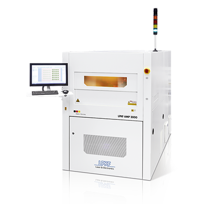
LPKF AMP 3000 장비 [사진=LPKF]
A. LTE 시대부터 지금까지 안테나 분야에서 가장 폭넓게 사용된 LDS(Laser Direct Structuring) 기술을 반도체 패키지에 응용한 ‘AMP(Active Mold Packaging) 3000’ 장비를 소개하고 싶습니다. 해당 장비는 반도체 RDL, 안테나온칩(Antenna-on-Chip), EMI 관리 그리고 열 관리 등에 활용할 수 있습니다.
Q. 향후 한국 시장에서의 목표는 무엇입니까?
A. PCB 관련 산업은 물론, 차세대 기술 파트너로서 전자, 디스플레이, 반도체, 자동차, 의료 등의 분야에서 국내 산업 생태계에서 중요한 역할을 하고자 합니다.
Comments
Related news
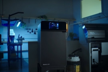
El Corporation, Formlabs 3D printer 'Fuse 1' exclusively supplied in Korea
EL Corporation will be the exclusive domestic supplier of Fuse1, Formlabs' new low-cost compact 3D printer. Fuse1 is a selective laser sintering (SLS) 3D printer scheduled for sale in May. Fuse1 can produce various 3D-printed objects using Nylon12 powder developed by Formlabs, making it suitable for multiple industry sectors.
2021.05.13by 강정규 기자
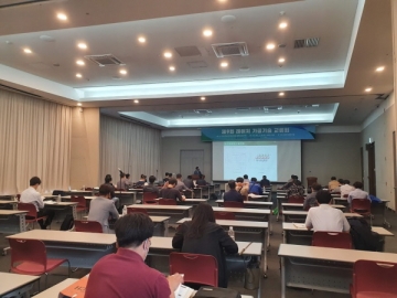
Korea Institute of Machinery and Materials, a gathering of laser processing technology experts
The Korea Institute of Machinery and Materials (President Park Sang-jin) held a "Laser Processing Technology Exchange Meeting," introducing the institute's corporate support programs, the Korea Industrial Complex Corporation's business support initiatives, Korea Maritime and Ocean University's laser workforce development project, and laser application technologies applicable to electric vehicles.
2021.05.26by 배종인 기자
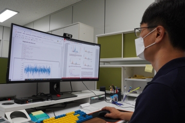
Deep learning technology that preemptively diagnoses manufacturing equipment failures has been developed
Current AI fault diagnosis technology only provides simple judgment information of normal or fault status, and fails to provide explanations and evidence for why faults are predicted. Accordingly, KIST has developed explainable AI-based equipment fault diagnosis technology in collaboration with POSTECH that captures fault symptoms of manufacturing equipment using deep learning technology and visually represents the causes and judgment criteria.
2021.08.02by 이수민 기자
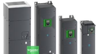
Schneider Aims for Building Energy Savings and Operational Stability with Next-Generation HVAC Drives
Schneider Electric has unveiled its next-generation HVAC drive product line 'Altivar HVAC'. The new product line's key features center on enhanced energy savings, system operational stability, and building management system integration. The products are divided into 'ATH200' for OEM and small equipment applications, and 'ATH600' for environments requiring continuous operation and advanced control. The company plans to expand the application scope from commercial buildings to facilities where HVAC system stability is critical, such as hospitals, airports, and data centers. The announcement includes over 30% energy savings, operation from -10°C to +60°C, Modbus and BACnet support, and compatibility with low global warming potential refrigerants.
2026.03.26by 명세환 기자
Ecolab Expands AI Data Center Cooling Business Through Acquisition of CoolIT
Ecolab has agreed to acquire CoolIT Systems, a liquid cooling company for AI data centers, for approximately $4.75 billion. The transaction is expected to close by Q3 2026, subject to regulatory approvals. CoolIT has been supplying direct-to-chip cooling-based coolant distribution units, cold plates, and manifolds, serving hyperscale data centers and colocation operators as customers. This acquisition is a measure to address the high-heat and high-density server environments created by AI proliferation. Ecolab plans to combine its water management and digital monitoring capabilities with CoolIT's hardware technology to expand its data center cooling business.
2026.03.26by 명세환 기자











