


Samsung Electronics Obtains 'Carbon Footprint' Certification for System Semiconductors
 Published2021.09.09 08:13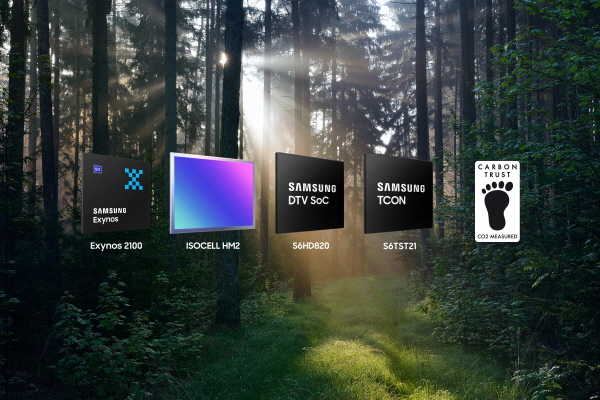
Samsung Electronics has received international environmental certification for system semiconductor products following its memory products.
Samsung Electronics has obtained Product Carbon Footprint (PCF) certification from The Carbon Trust (UK) for four types of high-performance system semiconductor products.
Product Carbon Footprint is a certification granted to products whose carbon emissions generated from production through disposal are calculated in accordance with the carbon footprint calculation standard (PAS 2050).
Utilities such as electricity, water, and gas required for product manufacturing, raw material production processes, and carbon emissions from transportation are evaluated according to strict international audit standards.
In particular, semiconductors undergo hundreds of complex manufacturing processes, and because the types and quantities of materials used are substantial, the certification process is considerably more rigorous.
The products for which Samsung Electronics has obtained Product Carbon Footprint certification this time are four types of high-performance system semiconductors: mobile SoC 'Exynos 2100', mobile image sensor 'ISOCELL HM2', Digital TV (DTV) SoC 'S6HD820', and Timing Controller (TCON) 'S6TST21'.
Samsung Electronics is reducing the volume of gases used in etching and deposition processes among semiconductor processes utilized in product manufacturing, and is enhancing the treatment efficiency of greenhouse gas decomposition equipment. Additionally, Samsung is minimizing carbon emissions by applying solutions for improving product power consumption efficiency.
Hugh Jones, Chair of The Carbon Trust Certification Committee, stated, "We are pleased to participate in Samsung Electronics' sustainable management activities," and added, "Product Carbon Footprint is an indicator that demonstrates Samsung Electronics' commitment to reducing carbon emissions to its customers."
Sung-dae Jang, Senior Executive Vice President of the Sustainable Management Office at Samsung Electronics' DS Division, said, "Samsung Electronics' environmentally friendly activities for sustainable management are being recognized globally," and noted, "Samsung Electronics will simultaneously expand the acquisition and reduction certification of Product Carbon Footprint for high-performance system semiconductors and will continue efforts to reduce carbon emissions."
Meanwhile, Samsung Electronics first received Product Carbon Footprint certification for memory products from The Carbon Trust in 2019, and obtained carbon reduction certification in 2020.
Additionally, in June 2021, Samsung received 'Carbon, Water, Waste Reduction' certification for all semiconductor business facilities and became the first in the industry to obtain the 'Triple Standard' label, expanding the scope of environmental certification to system semiconductor products.
Samsung Electronics has so far obtained Product Carbon Footprint certification from The Carbon Trust for a total of 14 products.

Comments
Related news
Samsung Electronics and Korea University Join Forces on Eco-Friendly Energy
Samsung Electronics and Korea University have signed a Memorandum of Understanding (MOU) for the establishment of an 'Eco-Friendly Energy Research Center,' entering into industry-academia collaboration for the development of eco-friendly home appliance solutions.
2021.09.01by 배종인 기자
Samsung Electronics Unveils 200-Mediapixel Image Sensor and Compact Dual-Pixel Image Sensor
Samsung Electronics has unveiled the ISOCELL HP1, a 200-megapixel mobile image sensor, and the ISOCELL GN5, an industry-leading dual-pixel image sensor with the smallest size. The HP1 is a product that implements 200 million pixels with 0.64 micrometer pitch in a 1/1.22-inch optical format size. The GN5 is an industry-leading smallest dual-pixel product that implements 50 million pixels with 1.0 micrometer pitch in a 1/1.57-inch optical format.
2021.09.02by 이수민 기자
.jpg)
Samsung Electronics Enhances Performance and Stability of New Micro SD Card Products
Samsung Electronics has launched a new microSD card product with enhanced performance and stability.
2021.09.08by 배종인 기자

Intel Unveils Next-Generation 'Core Ultra Series 3' and vPro Platform for Enterprise PCs
Intel has officially unveiled the "Intel Core Ultra Series 3" for next-generation enterprise PCs and the latest vPro platform, addressing a wide range of demands from enterprise notebooks to high-performance workstations.
2026.03.26by 배종인 기자

ROHM Launches ESD Protection Diode Compatible with High-Speed Interfaces of 10Gbps or Higher
Semiconductor specialist ROHM has developed the 'RESDxVx series' of ESD (electrostatic discharge) protection diodes capable of responding to next-generation high-speed data communication environments exceeding 10Gbps, simultaneously enhancing both signal quality maintenance required in high-speed interfaces and IC protection performance.
2026.03.26by 배종인 기자











