



[Technical Contribution] ADI's Frederik Dostal: "Increasing Loop Bandwidth and Reducing the Number of Output Capacitors"
 Published2021.10.18 17:02
AVP 기능, 낮은 부하 전압 높이고·높은 부하 전압 낮춰
출력 커패시터 구성·스위칭 레귤레이터 조절해서 최적화

 전원장치 출력 커패시터(흔히 세라믹 커패시터로서, 값은 100nF∼100μF 사이)는 비용이 들고, 자리를 차지하며, 때로는 공급 부족 문제 때문에 제때 구하기 힘들 때도 있다. 그래서 “어떻게 하면 출력 커패시터의 수와 크기를 최소화할 수 있을까?”하는 것이 설계자들이 수시로 하는 고민이다.
출력 커패시터가 미치는 영향으로 크게 두 가지를 들 수 있다. 출력 전압 리플에 미치는 영향과 부하 트랜션트가 발생했을 때 출력 전압에 미치는 영향이다.
그 전에 먼저, 출력 커패시터라는 용어부터 확인할 필요가 있다. 이것은 전원장치 출력에 사용되는 커패시터를 말한다.
그런데 FPGA 같은 전기 부하 역시 입력에 특정한 숫자의 커패시터들을 필요로 한다.
그림 1은 전원장치 설계와 부하로서 FPGA를 보여준다. 회로 보드 상에서 전압을 발생하는 측과 소비하는 측의 물리적 거리가 가까우면 전원장치 출력 커패시터와 부하측 입력 커패시터를 명확하게 구분하기가 어려울 수 있다.
이럴 때는 물리적 분리를 통해 구분을 할 수 있는데, 이렇게 하면 상당한 기생 인덕턴스(Llayout)가 발생할 수 있다.
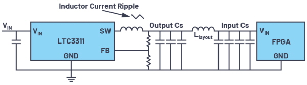
▲그림 1: LTC3311 스위칭 레귤레이터와 이에 연결된 FPGA의 출력 커패시터와 입력 커패시터.
전원장치 출력에서의 커패시터 구성이 스텝다운(벅) 스위칭 레귤레이터의 전압 리플을 결정한다. 출력 리플 전압은 인덕터 리플 전류에 출력 커패시터 임피던스를 곱한 것이라는 원칙이 여기에도 적용된다.

이 임피던스 ZCout은 커패시터들의 크기와 수뿐 아니라 등가 직렬 저항(ESR)과 등가 직렬 인덕턴스(ESL)도 포함한다. 전원장치 출력에 커패시터가 하나라면 이 공식을 아주 쉽게 적용할 수 있을 것이다.
하지만 그림 1에서처럼 다수의 커패시터들을 병렬로 사용하고, 레이아웃 때문에 직렬 인덕턴스(Llayout)가 발생하는 복잡한 경우라면 계산은 결코 간단치 않다.
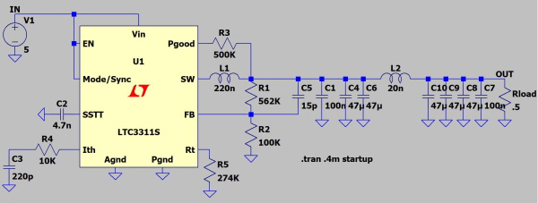
▲그림 2: LTspice를 사용하면 시스템의 전원장치 출력에 서로 다른 커패시터들을 시험해 볼 수 있다.
.jpg)
▲그림 3: LTpowerCAD를 사용해서 스위칭 레귤레이터의 제어 루프를 최적화하고 출력 커패시터의 수를 줄일 수 있다.
이러한 경우, LTspiceⓡ 같은 시뮬레이션 툴을 사용할 수 있다. 그림 2는 그림 1의 상황에 대해 신속하게 생성된 회로도를 보여준다. 개별 커패시터들에 대해 ESR과 ESL을 비롯해서 다양한 값들을 지정해볼 수 있다. 보드 레이아웃이 미치는 영향(Llayout 등)도 고려 사항에 포함할 수 있다. 그런 다음에 스위칭 레귤레이터 출력과 부하 입력에서 전압 리플을 시뮬레이트할 수 있다.
출력 커패시터는 부하 트랜션트 후에 출력 전압 오프셋에도 영향을 미친다. 이 영향 역시 LTspice를 사용해서 시뮬레이트할 수 있다. 특히 유의할 점은, 전원장치 제어 루프의 제어 속도와 출력 커패시터의 임피던스가 서로 연관되어 있다는 것이다. 전원장치 제어 루프가 빠를수록, 부하 트랜션트 후에 특정한 출력 제어 범위 이내로 유지하기 위해서 필요로 하는 출력 커패시터의 수를 줄일 수 있다.
LTC3311-1은 적응형 전압 포지셔닝(AVP)이라고 하는 기능을 제공한다. AVP 기능은 입력된 오차 전압 예산에 기반해서 루프 대역폭을 넓히는 방법으로서, 출력 커패시터의 수를 추가적으로 더 줄일 수 있다.
AVP 기능은 낮은 부하 조건일 때는 출력 전압을 약간 높이고 높은 부하 조건일 때는 출력 전압을 약간 낮춘다. 그럼으로써 부하 트랜션트가 발생했을 때 동적 출력 전압 변동이 허용 가능한 출력 전압 범위 이내에 있도록 한다.
아나로그디바이스(Analog Devices)의 LTpowerCADⓡ를 사용하면 제어 루프를 어떻게 최적화하고 출력 커패시터를 얼마나 줄일 수 있을지 알 수 있다. 그림 3은 제어 속도를 계산한 화면을 보여준다. 여기서는 부하 트랜션트에 이어서 전압 오버슈트가 발생하는 것을 볼 수 있다. 출력 커패시터 구성과 스위칭 레귤레이터 제어 루프 속도를 조절해서 최적화를 할 수 있다.
이렇게 최적화를 함으로써 전원장치에서 출력 커패시터의 수를 줄일 수 있고, 그 결과 비용과 보드 공간도 절약할 수 있다.
※ 위 글은 아나로그디바이스(Analog Devices, Inc.)의 프레데릭 도스탈(Frederik Dostal) FAE의 기고입니다.

Comments
Related news

ADI Unveils the ADRV9002, a Wide Dynamic Range RF Transceiver
ADI has launched the ADRV9002 RF transceiver, suitable for commercial and military applications. The ADRV9002 RF transceiver operates in the 30MHz to 6GHz frequency range and provides a receiver with a -150dBc/Hz dynamic range and a transmitter with high linearity.
2020.07.24by 명세환 기자
ADI Mass-Produces Digital Isolators Providing 10 Gbps Bandwidth
The ADN4624 digital isolator simplifies design and enables easy integration of isolation functionality for safety or data integrity. Meeting medical standards, it is a compact solution that reliably isolates Hi-Fi video and imaging links, precision analog front ends, and serial interconnects as an alternative to complex and specialized fiber optic solutions.
2021.07.01by 이수민 기자

ADI Presents Cost-Optimized Power Supply EMI Reduction Method
PCB layout configuration can be said to be decisive in the success or failure of power supply design. This is because it determines electromagnetic interference (EMI) and thermal performance. Switching power supply layout configuration is often overlooked until quite late in the design process. Therefore, using verified EMI reduction measures can ensure a reliable power supply.
2021.08.26by 이수민 기자

Intel Unveils Next-Generation 'Core Ultra Series 3' and vPro Platform for Enterprise PCs
Intel has officially unveiled the "Intel Core Ultra Series 3" for next-generation enterprise PCs and the latest vPro platform, addressing a wide range of demands from enterprise notebooks to high-performance workstations.
2026.03.26by 배종인 기자

ROHM Launches ESD Protection Diode Compatible with High-Speed Interfaces of 10Gbps or Higher
Semiconductor specialist ROHM has developed the 'RESDxVx series' of ESD (electrostatic discharge) protection diodes capable of responding to next-generation high-speed data communication environments exceeding 10Gbps, simultaneously enhancing both signal quality maintenance required in high-speed interfaces and IC protection performance.
2026.03.26by 배종인 기자











