



Keysight's full-scale push into the silicon photonics market
 Published2021.12.01 14:59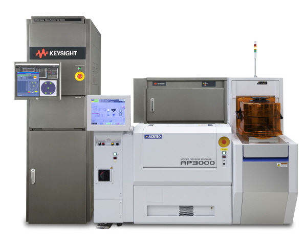
Semiconductor manufacturers can perform stable and repeatable testing.
Keysight Technologies is making a full-scale foray into the silicon photonics market by providing a fully automated, one-stop test solution that will enable semiconductor manufacturers to produce silicon photonics wafers faster.
Keysight Technologies, Inc. (NYSE: KEYS), a leading global provider of semiconductor test solutions, today announced that it has integrated its new NX5402A silicon photonics test system with Keysight's PathWave Semiconductor Test software technology, enabling semiconductor manufacturers to rapidly deliver silicon photonics wafers with reliable and repeatable test capabilities.
Silicon photonics is one of the key emerging technologies addressing the demand for higher data rates and increasing Internet traffic.
The primary application area for silicon photonics is the data center market driven by big data and cloud applications, but it is also expected to find use in other areas including healthcare, automotive LiDAR (Light Detection and Ranging), optical computing, and quantum computing.
According to Yole Développement, a global semiconductor research firm, the overall silicon photonics market size is expected to reach $3.9 billion by 2025.
Accordingly, many manufacturers are considering silicon photonics manufacturing.
On the other hand, fully automated webThere is no commercially available silicon photonics test equipment suitable for mass production using an Epher Prober.
Additionally, silicon photonics testing requires a variety of sensitive and accurate measurements.
Enterprises and system integrators are seeking ways to optimize and maintain their systems due to complex and inefficient communications across multiple vendors.
“To proactively address the growing market demand for silicon photonics, Keysight is pleased to announce the first test solution for the silicon photonics high-volume production market,” said Mr. Shinji Terasawa, vice president and general manager of Keysight’s Wafer Test Solutions Group. “The NX5402A test system is the first solution to combine Keysight’s expertise in electrical and optical measurements with Keysight’s fiber alignment and positioning system integrated by PathWave Semiconductor Test software.”

Comments
Related news

Keysight Korea Hosts 'Keysight World 2021'
Keysight Korea will host 'Keysight World 2021' online from October 12-14, introducing a wide range of solutions covering key technology areas including digital transformation, connectivity, and security.
2021.10.05by 배종인 기자
Keysight Launches State-of-the-Art Engineering Education Hub
Keysight Technologies provides educational resources covering a wide range of cutting-edge technologies for students, engineers, and business leaders, positioning itself as the latest engineering education hub.
2021.10.06by 배종인 기자

Keysight Korea Appoints Lee Seon-woo as New CEO
Keysight Technologies, a global electronic test and measurement specialist, has appointed Lee Sun-woo, Executive Director of the Communications Solutions Division at Keysight Korea, as Representative Director and President of Keysight Korea, effective November 1st.
2021.11.03by 명세환 기자

Intel Unveils Next-Generation 'Core Ultra Series 3' and vPro Platform for Enterprise PCs
Intel has officially unveiled the "Intel Core Ultra Series 3" for next-generation enterprise PCs and the latest vPro platform, addressing a wide range of demands from enterprise notebooks to high-performance workstations.
2026.03.26by 배종인 기자

ROHM Launches ESD Protection Diode Compatible with High-Speed Interfaces of 10Gbps or Higher
Semiconductor specialist ROHM has developed the 'RESDxVx series' of ESD (electrostatic discharge) protection diodes capable of responding to next-generation high-speed data communication environments exceeding 10Gbps, simultaneously enhancing both signal quality maintenance required in high-speed interfaces and IC protection performance.
2026.03.26by 배종인 기자











