



[Op-Ed] ADI Engineer Hakan Wuenlu – “ICs with Overvoltage Protection OTT Are the Best”
 Published2021.12.16 14:13
OTT amplifier withstands a maximum differential input voltage of 80V
1% resistance optimal, helps minimize voltage drop range
 The potential for high voltage generation is always a concern in industrial applications. Finding ways to protect circuits from high voltage has always been, and will continue to be, a critical task for developers. This design tip shows how developers can achieve this using Over-The-Top® (OTT) amplifiers.
Sometimes, even in industrial applications, voltages higher than the system power supply are generated. While the potential is not as high as in automotive electronics, it can be higher than typical system voltages.
Some system voltages can be too high to use many standard operational amplifiers. This poses a significant problem for the analog front end (AFE). For example, if the voltage is high, the internal input diode of a typical amplifier may turn on.
The longer this condition persists, the higher the likelihood of malfunctions or even breakdowns.
In such cases, developers can take corresponding preventive measures, for example, by using an external protection circuit along with an external diode or resistor.
However, using separate components like this requires additional board space and can be accompanied by disadvantages such as leakage current, additional capacitance, and noise. For this reason, an integrated IC solution equipped with OTT technology can be the best choice.
■ How OTT Works
To aid understanding, let's take a look inside the latest generation ADA4098-1 or ADA4099-1. Each of these OTT operational amplifiers has two input stages.
The first is a common emitter differential consisting of a PNP transistor that operates on an input signal between a negative power supply (-VS) and a positive power supply (+VS) up to about 1.25V lower.
The second is a common-base input stage consisting of an additional PNP transistor that operates with an input signal where the common-mode voltage is +VS ~ 1.25V or higher. An example of the internal circuit is shown in Figure 1.
The first stage is designed with transistors Q1 and Q2, and the second stage consists of transistors Q3 to Q6.
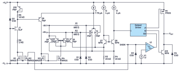
▲Figure 1. Brief internal structure (latest generation ADA4098-1)
Therefore, these input stages provide two distinct but complementary operating ranges. The offset voltages of the two input stages are strictly trimmed and provided in the datasheet.
When the input common mode voltage approaches +VS, the second stage is activated and the operational amplifier enters OTT mode. This state can be a case of overvoltage in various applications.
For example, in the case of high-side current measurements, the voltage may exceed the system power potential due to parasitic or load-related influences, even if it is transient.
A typical amplifier accepts signal voltage up to the power supply voltage range. If the input far exceeds this range, the internal diode typically turns on, and a significant current flows through the diode.
Depending on the signal voltage and current, these spikes can interfere with the operation of the amplifier or, in the worst case, cause failure in the integrated circuit.
Unlike typical operational amplifiers that experience these problems, OTT amplifiers can withstand differential input voltages of up to 80V.
In this state, the output level saturates with the positive power supply (+VS). In this state, the output can sink or supply current within the datasheet limits. When the input returns to the normal operating range (-VS to +VS), the output level also returns to the typical linear range without compromising or degrading DC accuracy. This case is similar to a common mode voltage of up to 70V.
■ Application Examples and Tips for Amplifiers Using OTT Technology
Several examples of current measurements can be seen in Figure 2. While the ADA4098-1 is a low-power version, the ADA4099-1 has a higher bandwidth and a higher voltage rise rate.
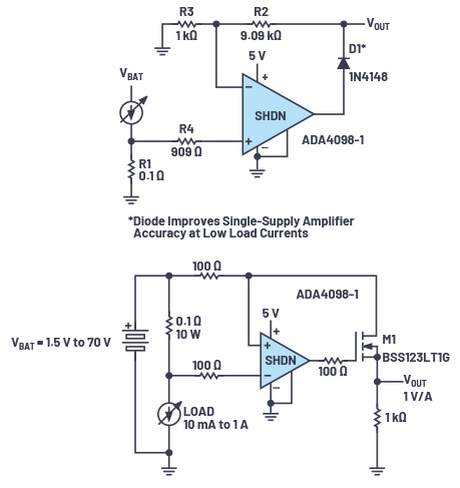
▲Figure 2. Current measurement example of ADA4098-1
In low-side measurements, the gain comes from resistors R2 and R3. Diode D1 improves single-power accuracy at low load currents.
In high-side current measurements, the 1kΩ and 100Ω (top) resistors are critical to the gain. The resistors at the amplifier input provide a filtering function above all else. In this case, a 1% resistor is optimal. Since the possible input bias current causes a voltage drop across these resistors, a strict tolerance like 1% here can help minimize the voltage drop range.
The output of the ADA4098-1 can swing rail-to-rail under no-load conditions within 45mV of the two power supplies. The output can source 24mA and sink 35mA. The amplifier is internally compensated and can drive a load capacitance of 200pF (minimum). The amplifier's capacitive load driving capability can be extended by inserting a 50Ω series resistor between the output and a higher capacitive load.
If the output VOUT drives the circuit at a lower potential and this downstream circuit has a protection diode for its own voltage rail, it is reasonable to place a resistor at VOUT. This limits the current that can flow to the downstream circuit.
The ADA4098-1 has a dedicated SHDN pin that places the amplifier in a very low shutdown state when the pin is asserted to high. Logic high is defined as a voltage of 1.5V or higher applied to the SHDN pin relative to the -VS pin. This places the VOUT pin in a high impedance state. Alternatively, removing positive power can effectively put the amplifier into a low-power state. In both of these off modes, OTT remains enabled, and voltages up to 70V can be applied to the input pin via -VS.
In addition to current or power measurement, another use for the OTT amplifier is as a sensor front end or a 4mA to 20mA current loop. Further information, additional application examples, and calculations can be found in the datasheet.
■ ADI 5th Generation OTT Amplifier Provides the Latest Overvoltage Protection from Lab to Circuit Design
So far, we have examined how over-the-top amplifiers provide protection against overvoltage. By incorporating intelligent and precise internal circuitry, OTT amplifiers offer both robustness and precision.
Analog Devices' 5th generation OTT amplifiers provide the latest overvoltage protection from the laboratory to circuit design. OTT operational amplifiers such as the ADA4098-1 and ADA4099-1 achieve lower offset error and noise values while providing higher voltage tolerances above the rail.
※ About the Author: Hakan Uenlue, Senior Field Application Engineer (FAE) at Analog Devices, Inc., received his Master's degree in Electrical and Electronic Engineering from the University of Stuttgart. After working as a hardware developer and field application engineer, I joined Analog Devices in 2015.

Comments
Related news

ADI Expands Linux Distributions… Supports 1,000 Device Drivers
Analog Devices has announced Kuiper Linux, a Raspberry Pi/Debian-based distribution that supports over 1,000 device drivers with Linux distribution expansion, marking its full commitment to supporting high-performance solution development.
2021.12.01by 강정규 기자
ADI Extends Battery Life with Lowest Standby Current
Analog Devices (ADI) has introduced essential analog nanopower uSLIC modules that extend battery life in space-constrained applications with ultra-low quiescent current.
2021.12.06by 강정규 기자

ADI Announces RadioVerse® SoC Series
Analog Devices (ADI) is advancing 5G wireless efficiency and performance through a new SoC.
2021.12.10by 강정규 기자

Intel Unveils Next-Generation 'Core Ultra Series 3' and vPro Platform for Enterprise PCs
Intel has officially unveiled the "Intel Core Ultra Series 3" for next-generation enterprise PCs and the latest vPro platform, addressing a wide range of demands from enterprise notebooks to high-performance workstations.
2026.03.26by 배종인 기자

ROHM Launches ESD Protection Diode Compatible with High-Speed Interfaces of 10Gbps or Higher
Semiconductor specialist ROHM has developed the 'RESDxVx series' of ESD (electrostatic discharge) protection diodes capable of responding to next-generation high-speed data communication environments exceeding 10Gbps, simultaneously enhancing both signal quality maintenance required in high-speed interfaces and IC protection performance.
2026.03.26by 배종인 기자











