


A new semiconductor that doesn't generate heat is emerging.
 Published2022.02.07 14:58
▲Professor Park Kyung-deok's research team (far left). Below are co-first authors Lee Hyeong-woo (left) and Koo Yeon-jeong (right).
Expectations for exciton-based semiconductors and optical communication devices
A method for controlling exciton particles without loss has been developed for the first time in the world, raising expectations that it will be possible to develop semiconductors that do not generate heat in the future by utilizing excitons instead of electrons.
UNIST announced on the 7th that Professor Kyung-Deok Park's team in the Department of Physics has developed the world's first technology that can control exciton particles (quasiparticles) without loss.
The development of next-generation semiconductor chips has gained momentum with the development of technology that can freely control high-efficiency excitons.
An exciton is a particle that occurs within an insulator or semiconductor material. It is electrically neutral because it is composed of a negatively charged electron and a positively charged hole.
This property allows for faster, less heat-intensive semiconductor chips to be created by using excitons instead of electrons.
As more devices are integrated to improve chip performance, unnecessary electric field interference occurs, but excitons, which are electrically neutral, do not cause such interference even when devices are integrated.
On the other hand, exciton particles have the problem of being easily lost. To create exciton-based semiconductor chips, the semiconductor material must be mechanically deformed. However, if the deformation is insufficient, external factors such as heat can cause the exciton particles within the material to disappear. Furthermore, if the bending is too strong, the material itself can be permanently damaged.
The research team overcame this limitation by creating a device with a nano-gap structure (nano-gap device).
It is a form in which a thin two-dimensional semiconductor material is stretched over a gap structure and rolled into the gap.
The length of this gap is extremely short (unit length), on the order of hundreds of nanometers (nm, one-hundred-millionth of a meter), which can reduce loss. To reduce exciton loss, the strain (the amount of deformation per unit length) of the two-dimensional semiconductor material must be large.
In this state, if the research team presses the tip of the 'active probe-enhanced photoluminescence nanomicroscope' previously developed, the behavior of exciton particles generated within the two-dimensional semiconductor material can be more efficiently controlled.
The tip of the 'active probe-enhanced photoluminescence nanomicroscope' has a narrow cross-sectional area of about 10 nanometers, so the pressure (force applied per unit area) applied to two-dimensional semiconductor materials can be increased to the gigapascal (GPa) level.
The higher the pressure applied, the higher the strain. Another advantage of this technology is that when the probe is removed, the applied mechanical deformation is restored to its original state.
The research team also theoretically proved this control principle.
This study was led by Lee Hyeong-woo and Gu Yeon-jeong, graduate students in the Department of Physics at UNIST.
The research team explained, “Not only have we elucidated the exciton behavior phenomenon at the nanoscale for the first time in the world through theory and experiment, but we have also proposed a solution to the efficiency problem, which has been a limitation of existing exciton behavior control research,” and “This is a new study that breaks the conventional wisdom of existing exciton behavior control research.”
Professor Park Kyung-deok said, “The exciton-based device presented this time is a dynamic device that can be freely controlled,” and expressed his expectations, saying, “It can also be used in research on the development and performance improvement of various exciton-based nano-semiconductors and optical communication devices.”
Meanwhile, exciton particles are also advantageous for ultra-high-speed optical communications. This is because there is no need to convert digital information into a separate optical signal due to the characteristic of emitting light when electrons and holes bound by electrostatic force combine.
The nano-gap devices used in this study were produced by Vice President Joo-hyuk Joo's research team at Samsung Electronics and Professor Hyung-ryeol Park's team from the Department of Physics at UNIST. Professor Ki-gang Kim's team from the Department of Energy Science at Sungkyunkwan University participated in the production of the two-dimensional semiconductor material.
The research results were published in the international academic journal 'Science Advances' on February 4, and the research was conducted with support from the National Research Foundation of Korea, UNIST, and IBS.
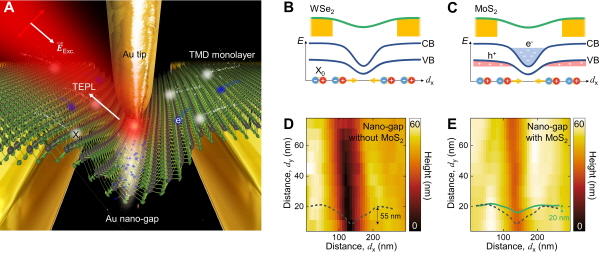
▲A diagram depicting observation of nanoscale exciton behavior using a probe-enhanced photoluminescence nanomicroscope.

Comments
Related news

UNIST, AI World Stage ‘Top’ Recognition
A graduate student Yun Tae-hyun from UNIST's Graduate School of Artificial Intelligence (advisor: Prof. Lim Sung-bin) achieved the top position in the student category at a prestigious global artificial intelligence conference competition. The achievement was recognized for delivering the highest program performance in an emerging field that has recently attracted significant academic attention.
2021.12.06by 배종인 기자

UNIST Challenges Development of 35% Efficiency Super Solar Cells
UNIST challenges the development of a super solar cell achieving 35% efficiency over five years, contributing to carbon neutrality and the advancement of Korea's photovoltaic industry.
2021.12.22by 배종인 기자
UNIST and Yonsei Medical Center Join Hands for Smart Healthcare
UNIST (President Yong-Hoon Lee) and Yonsei University Health System (Director Dong-Seop Yoon) will strengthen research capabilities and contribute to advances in medical technology through the joint promotion of research in the smart healthcare field.
2022.01.10by 배종인 기자

Intel Unveils Next-Generation 'Core Ultra Series 3' and vPro Platform for Enterprise PCs
Intel has officially unveiled the "Intel Core Ultra Series 3" for next-generation enterprise PCs and the latest vPro platform, addressing a wide range of demands from enterprise notebooks to high-performance workstations.
2026.03.26by 배종인 기자

ROHM Launches ESD Protection Diode Compatible with High-Speed Interfaces of 10Gbps or Higher
Semiconductor specialist ROHM has developed the 'RESDxVx series' of ESD (electrostatic discharge) protection diodes capable of responding to next-generation high-speed data communication environments exceeding 10Gbps, simultaneously enhancing both signal quality maintenance required in high-speed interfaces and IC protection performance.
2026.03.26by 배종인 기자











