



Development of 2D Carbon Allotropes with Semiconductor Properties
 Published2022.05.19 11:21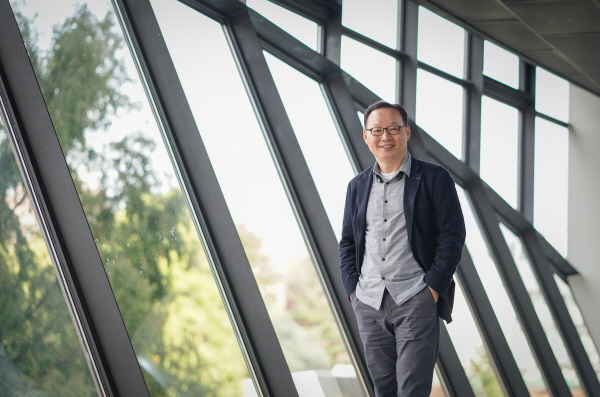
▲ Lee Hyo-young, Deputy Director of IBS Research Group
A two-dimensional carbon allotrope with semiconductor properties has been developed, raising expectations that it will be utilized in various fields such as optoelectronics, catalysts, and sensors in the future.
The research team led by Deputy Director Lee Hyo-young (Professor at Sungkyunkwan University) of the Institute for Basic Science (IBS, President Noh Do-young)'s Center for Nanostructure Physics (Director Lee Young-hee) announced on the 19th that they have developed 'Holygraphine,' a new two-dimensional carbon allotrope with semiconductor properties.
The research team expects that by synthesizing a material that compensates for the shortcomings of graphene, which is difficult to implement as a semiconductor, it can be utilized in various fields such as optoelectronics, catalysts, and sensors.
Representative carbon allotropes are diamond and graphite. Various carbon allotropes discovered in modern times, such as graphene, fullerene, and carbon nanotubes, are revolutionizing nanomaterial science.
In particular, graphene has garnered attention as a dream material because its electron mobility reaches 140 times that of silicon and its strength reaches 200 times that of steel.
On the other hand, graphene has limitations in being used as a semiconductor because it lacks a bandgap. A bandgap must exist to be utilized as a semiconductor that allows electricity to flow at times and not at others. To overcome the limitations of graphene, research is actively underway to find a new type of two-dimensional carbon allotrope that has a fast charge transfer rate while also being capable of bandgap tuning.
Research results continue to show that creating holes in graphene through physical or chemical methods hinders the flow of current, thereby enabling bandgap tuning. This material is called "holey graphene." However, it is difficult to achieve desired properties in holey graphene because the size and distribution of the "holes" are not uniform.
Accordingly, instead of using the conventional method of creating holes in graphene, the research team applied a method of generating regular holes by newly synthesizing carbon materials from the atomic level. The team named this synthesized material 'Holygraphine'.
Hollygraphine is characterized by benzene rings (rings composed of 6 carbon atoms) being alternately connected by triple bonds (C≡C), and by patterns of hexagonal and octagonal rings being composed in equal proportions.
The research team synthesized an ultrathin two-dimensional semiconductor, Hollygraphine, between the interfaces of two solvents composed of water and dichloromethane using a monomer of '1,3,5-tribromo-2,4,6-triethylbenzene' that underwent a six-step reaction.
The band gap of holographine is 1.1 eV, which is similar to the silicon band gap (1.12 eV). In addition, the charge transfer speed is similar to that of graphene (predicted to be 104 cm²v⁻¹s⁻¹ by calculation), confirming its suitability as a semiconductor material.
Hollygraphine possesses excellent semiconductor properties and triple and conjugated bond structures, so it is expected to be applicable in various fields such as optoelectronics, catalysts, and sensors.
“This research achievement presents the possibility of designing and synthesizing a new type of two-dimensional carbon allotrope by synthesizing an ultrathin single crystal for the first time,” said Deputy Research Director Lee Hyo-young. “This research on carbon allotropes will contribute to ushering in a next-generation semiconductor era that goes beyond silicon.”
The results of this study were published online on May 19 in Matter (IF 15.589), a sister journal of Cell.

Comments
Related news

IBS celebrates its 10th anniversary with a variety of events, including lectures by Nobel laureates.
The Institute for Basic Science (IBS, Director No Do-young) has organized various science concerts, including lectures by Nobel Prize laureates, to commemorate its 10th anniversary since its establishment.
2021.11.08by 배종인 기자
.jpg)
IBS produces hydrogen four times cheaper and for more than twice as long.
A new catalyst that produces hydrogen from any water has been developed and is drawing expectations to contribute to environmentally friendly hydrogen production.
2021.11.23by 배종인 기자
IBS Discovers Next-Generation Magnetic Semiconductor Materials
Domestic researchers have discovered a next-generation magnetic semiconductor material for the first time globally, and it is expected to play an important role in implementing spin information devices that are robust against external noise and free from information loss.
2021.11.25by 배종인 기자
Schneider Aims for Building Energy Savings and Operational Stability with Next-Generation HVAC Drives
Schneider Electric has unveiled its next-generation HVAC drive product line 'Altivar HVAC'. The new product line's key features center on enhanced energy savings, system operational stability, and building management system integration. The products are divided into 'ATH200' for OEM and small equipment applications, and 'ATH600' for environments requiring continuous operation and advanced control. The company plans to expand the application scope from commercial buildings to facilities where HVAC system stability is critical, such as hospitals, airports, and data centers. The announcement includes over 30% energy savings, operation from -10°C to +60°C, Modbus and BACnet support, and compatibility with low global warming potential refrigerants.
2026.03.26by 명세환 기자
Ecolab Expands AI Data Center Cooling Business Through Acquisition of CoolIT
Ecolab has agreed to acquire CoolIT Systems, a liquid cooling company for AI data centers, for approximately $4.75 billion. The transaction is expected to close by Q3 2026, subject to regulatory approvals. CoolIT has been supplying direct-to-chip cooling-based coolant distribution units, cold plates, and manifolds, serving hyperscale data centers and colocation operators as customers. This acquisition is a measure to address the high-heat and high-density server environments created by AI proliferation. Ecolab plans to combine its water management and digital monitoring capabilities with CoolIT's hardware technology to expand its data center cooling business.
2026.03.26by 명세환 기자











