



UNIST Makes Semiconductor Patterning as Simple as Printing a Photo
 Published2022.10.04 11:03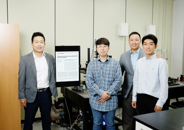
▲ Participants in this study (from left): Professor Lee Ji-seok, Researcher Jeong Sang-gyun, Professor Son Jae-seong, and Researcher Baek Seong-heon
Development of Low-Cost, High-Efficiency Inorganic Optical Printing Technology
UNIST (President Lee Yong-hoon) has developed a technology that enables semiconductor patterning as simply as printing a photograph, raising expectations that future patterning could be realized at low cost and with simple fixed methods.
A research team led by Professors Son Jae-seong and Lee Ji-seok at UNIST recently announced the development of a 'metal chalcogenide ink' that hardens when exposed to light (photocurable) and an optical printing process utilizing it.
Metal chalcogenides are inorganic materials that can play a pivotal role in various devices due to their luminescent and electrical properties, and a way has now been opened to easily pattern them. Using this technology, the research team succeeded in fabricating two-dimensional (2D) and three-dimensional (3D) structures and 'micro thermoelectric devices,' proving its potential as a 'patterning technology for inorganic materials' to replace existing processes.
Conventional material patterning utilized photolithography, which etches the material with light, or technology that etches circuits using lasers and electron beams (e-beams). However, such processes are expensive, complex, and time-consuming. As an alternative, 'optical 3D printing technology' that uses light to build up materials has emerged, but most of these contain photocurable polymers (organic materials), which has the problem of degrading the properties of the materials.
To solve this problem, the research team synthesized a polymer-free 'photocurable inorganic ink' and developed 'inorganic material optical printing technology' by integrating it into a Digital Light Processing (DLP) printing process. Among various inorganic materials, they utilized metal chalcogenides and 2D transition metal dichalcogenides, which have recently been gaining attention as semiconductor materials.
"Optical printing technology can uniformly produce high-resolution patterns over a large area," explained Jae-Sung Son, a professor in the Department of Materials Science and Engineering at UNIST. "It is a technology that enables the fabrication of two-dimensional and three-dimensional structures through a relatively low-cost, simple process."
Unlike conventional methods, the newly developed optical printing process uses only 'pure inorganic ink.' Additionally, by utilizing a DLP printing process that builds up ink to a nanometer thickness, it is possible to fabricate semiconductor material structures with significantly reduced manufacturing costs and time.
Generally, optical printing processes involving inorganic materials use photocurable polymer composites containing inorganic additives as ink. In this case, polymers remain inside the structure after the process, impairing electrical properties, but this technology solves this by using only 'pure inorganic materials'. After synthesizing a metal chalcogenide precursor (ChaM) solution, a photoacid generator (PAG) was added to impart photocuring properties suitable for optical printing.
Professor Lee Ji-seok of the Department of Energy and Chemical Engineering at UNIST said, “It is a precise technology that can control printed structures down to the tens of nanometers without a polymer support,” and added, “It is an important technology that not only dramatically improves existing optical 3D printing processes but also overcomes the limitations of printing materials to directly incorporate various inorganic materials into the printing process.”
The 2D and 3D structures produced through this process demonstrated high resolution and uniformity, and also showed the potential for large-area printing and 3D stacking. Furthermore, a micro thermoelectric generator was fabricated using an optical printing process, proving its potential for application in the energy field.
Baek Seong-heon, the first author and a researcher in the integrated master's and doctoral program in Materials Science and Engineering at UNIST, expressed his expectation that "depending on the various functional materials, it could be applied to semiconductor devices or optoelectronic devices." Meanwhile, Jeong Sang-gyun, a co-first author and a researcher in the integrated master's and doctoral program in Energy and Chemical Engineering at UNIST, stated, "Since it does not use the 'photomask' required in photolithography, it is not restricted by shape or size, allowing for free application in various fields."
This study was published in the online edition of the world-renowned scientific journal Nature Communications on September 7. The research was supported by the National Research Foundation of Korea’s Challenge Materials Technology Development Program, Future Materials Discovery, and Mid-Career Researcher Support Program.

Comments
Related news
1nm semiconductors are just around the corner
Researchers at UNIST (President Lee Yong-hoon) have brought the development of 1-nanometer semiconductors within reach by reducing the interface between semiconductor and metal within semiconductor devices to '1 nanometer (nm, one billionth of a meter)' or less.
2022.09.05by 배종인 기자
UNIST Develops New Metasurface for 6G Communications
A special device material with versatile active characteristics for use in 6G mobile communications utilizing 'terahertz (THz) bandwidth' has been developed and is expected to be utilized in future terahertz and infrared hybrid communications.
2022.09.06by 배종인 기자
KETI Wins 1st Place in AI Competition for UNIST
Ulsan National Institute of Science and Technology (UNIST) claimed first place honors at the Artificial Intelligence Competition for Sustainable Energy Utilization.
2022.09.16by 배종인 기자

Intel Unveils Next-Generation 'Core Ultra Series 3' and vPro Platform for Enterprise PCs
Intel has officially unveiled the "Intel Core Ultra Series 3" for next-generation enterprise PCs and the latest vPro platform, addressing a wide range of demands from enterprise notebooks to high-performance workstations.
2026.03.26by 배종인 기자

ROHM Launches ESD Protection Diode Compatible with High-Speed Interfaces of 10Gbps or Higher
Semiconductor specialist ROHM has developed the 'RESDxVx series' of ESD (electrostatic discharge) protection diodes capable of responding to next-generation high-speed data communication environments exceeding 10Gbps, simultaneously enhancing both signal quality maintenance required in high-speed interfaces and IC protection performance.
2026.03.26by 배종인 기자











