


ETRI Commercializes Light Source Device Capable of 25Gbps/30km Transmission
 Published2023.03.02 08:57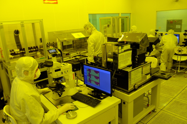
▲ ETRI researchers conducting the process for field-absorption modulation light source devices and optical modules at ETRI's semiconductor FAB.
We will expand the 100Gbps wired network market, including 5G networks and data centers.
Domestic researchers and small and medium-sized enterprises have joined forces to successfully commercialize, for the first time in Korea, a light source device capable of transmitting 25 billion bits per second over long distances through fiber optic cables.
The Korea Electronics and Telecommunications Research Institute (ETRI) announced that it has succeeded in commercializing a field-absorbing modulated light source device capable of transmitting data over 30 km at a speed of 25 Gbps, in collaboration with LDIS, a company specializing in optical communications.
With this, a technological foundation has been laid to respond to the surge in data traffic and the demand for 5G mobile communication networks.
In order to accommodate high-capacity communication services such as 5G mobile communication, light sources have been directly modulated and turned on and off using a current application method.
However, this method had limitations such as delays in the current charging and discharging times of the light source element, resulting in reduced modulation speed and degraded signal quality.
ETRI developed a field-absorbing modulated light source device to solve these problems.
This method controls the light output intensity by instantaneously absorbing light depending on the voltage applied to the output terminal of a light source element that emits light at a constant intensity.
Through this, the research team [signaled] on/off signals to the output terminal of the light source device It was fabricated in an integrated form of a viable electric field absorption modulator (EAM).
It has become possible to resolve the problems of reduced modulation speed and signal quality degradation, which were issues with the existing direct modulation method.
Currently, only a few companies worldwide are able to supply field-absorption modulated light source devices, so this technology development has made it possible to break free from dependence on overseas imports in the future.
The research team evaluated this research result as a successful fusion of the compound semiconductor technology that ETRI has pioneered in its R&D foundry and the mass production technology of a domestic company specializing in compound opto-semiconductors.
The composition of the In-Al-Ga-As (Indium-Aluminum-Gallium-Arsenic) compound, which was advantageous in terms of light source device performance such as optical output intensity and modulation speed at existing high temperatures but had low reliability, was changed to an In-Ga-As-P (Indium-Gallium-Arsenic-Phosphorus) composition.
The strategy modified to be advantageous for rapid commercialization considerations and securing initial reliability in the company's future mass production process proved effective.
To date, field-absorbing modulated light source devices produced in the mass production process of LDIS Co., Ltd. are capable of transmitting 25Gbps not only at room temperature but also at a high temperature of 55℃.
In addition, a modulation speed of 100Gbps, applicable to internal data center networks, has been secured.
It is on par with global competing products.
Eldis Co., Ltd. aims to first increase the mass production yield of 25Gbps-class products to supply them to domestic and international 5G markets, and to launch 100Gbps-class products in the first half of next year.
In the future, ETRI and LDIS Co., Ltd. plan to continue cooperating to strengthen product competitiveness by improving the performance and diversifying field-absorbing modulated light source devices.
We also plan to focus on evaluation technologies for post-semiconductor processes, such as characteristics and reliability, as well as performance optimization through the application of optical modules.
ETRIJong-jin, Head of the Optical Packaging Research Lab, stated, “I believe this is highly significant as it is an excellent example where the research team’s prior research achievements led to technology commercialization. We will provide support through continuous cooperation during the commercialization process to ensure it becomes the world’s best product.”
ETRI’s Han Young-tak, Head of Technology Transfer, also stated, “For compound opto-semiconductors, which are highly sensitive to process variables, stable foundry operation is key. We will strive to ensure that the research team’s foundry produces world-class results.”
Jo Ho-seong, CEO of LDIS, explained, “The government’s policies to foster the materials, parts, and equipment industries are gradually bearing fruit. Building on the success of localizing high-value-added light sources like EML, continuous support from government-funded research institutes and the government is necessary to enable domestic compound optoelectronic semiconductor companies to bridge the technological gap with the outside world and achieve greater results, such as entering overseas markets with domestically produced light source devices.”
This achievement was made through the Ministry of Science and ICT's projects 'Low-power On-Board integrated 400Gbps optical transceiver engine technology for increasing data center communication capacity' and 'Development of 800Gbps optical transceiver for data center internal networks'.

Comments
Related news
ETRI Distributes Core AI Semiconductor Software for Free
ETRI has developed and disclosed core technologies to shorten the development time and reduce costs for AI semiconductor design.
2022.02.03by 김예지 기자
.jpg)
ETRI, Global Cooperation in SiC and 6G Semiconductors
The Electronics and Telecommunications Research Institute (ETRI) has agreed to cooperate with the Korea Advanced Institute of Science and Technology (KAIST) and U.S.-based Coherent on the development of next-generation semiconductor materials and components technology as well as global industrialization efforts.
2022.12.12by 배종인 기자
ETRI Develops Ultra-High-Speed Optical Input/Output Semiconductor Using Light
The Electronics and Telecommunications Research Institute (ETRI) has developed a silicon photonics optical semiconductor chip and related modules capable of transmitting data at 100 gigabits per second (100Gbps) in next-generation data centers and high-performance computing networks.
2022.12.22by 배종인 기자

Intel Unveils Next-Generation 'Core Ultra Series 3' and vPro Platform for Enterprise PCs
Intel has officially unveiled the "Intel Core Ultra Series 3" for next-generation enterprise PCs and the latest vPro platform, addressing a wide range of demands from enterprise notebooks to high-performance workstations.
2026.03.26by 배종인 기자

ROHM Launches ESD Protection Diode Compatible with High-Speed Interfaces of 10Gbps or Higher
Semiconductor specialist ROHM has developed the 'RESDxVx series' of ESD (electrostatic discharge) protection diodes capable of responding to next-generation high-speed data communication environments exceeding 10Gbps, simultaneously enhancing both signal quality maintenance required in high-speed interfaces and IC protection performance.
2026.03.26by 배종인 기자











