



[Technical Contribution] ADI's Frederic Dostal: Why Smaller is Better
 Published2023.05.22 11:11
PCB 출력 커패시터 같은 외부부품 수 최소화
LTM8074, 40V 입력전압·1.2A 출력전류 지원
 전원 모듈은 수년 전부터 시장에서 사용되어 왔다. 전원 모듈은 단일 패키지 제품으로서, 대개는 보드 상에 간단히 솔더링 할 수 있고 입력 전압을 특정한 출력 전압으로 변환하는 작업을 수행하는 스위치 모드 전원공급장치(SMPS)이다.
스위칭 레귤레이터 IC가 칩 상에 컨트롤러와 전력 스위치만 통합하고 있는 것과 달리, 전원 모듈은 다수의 수동 소자들까지 통합한다.
일반적으로 인덕터를 통합했을 때 ‘전원 모듈’이라는 용어를 사용한다.
그림 2에서는 스위치 모드 스텝다운 컨버터(벅 토폴로지)에 필요한 소자들을 보여준다. 그림에서 점선은 스위칭 레귤레이터 IC와 전원 모듈을 구분해서 보여준다. 이러한 모듈을 위한 전압 변환 회로 개발은 전원 모듈 회사가 담당하기 때문에, 사용자는 전원공급장치 전문가가 될 필요가 없다.
또 다른 장점이 있다. 이 모듈의 높은 통합 수준 덕분에 SMPS의 크기를 극히 소형화할 수 있다는 것이다.
■ 더 정숙하고 작은 DC-DC 레귤레이션 구현
스위칭 레귤레이터는 비교적 높은 주파수에서 높은 dI/dt로 동작하기 때문에, 본질적으로 방사 EMI를 발생한다. 그런데 EMI 적합성 준수는 의료용 장비, RF 트랜시버, 시험 및 계측 시스템에서 신호 처리와 관련해서 의무 조항이자 중요한 설계 과제이다.
예를 들어서 어떤 시스템이 EMI 요건을 충족하지 못하거나, 혹은 스위칭 레귤레이터가 고속 디지털 또는 RF 신호 무결성에 영향을 미친다면, 디버깅이나 설계 변경으로 인해 설계 일정이 길어질 뿐만 아니라 재검증 작업 때문에 비용이 늘어날 것이다. 뿐만 아니라 DC-DC 스위칭 레귤레이터가 잡음에 민감한 부품이나 신호 배선에 가깝게 배치되는 밀집된 PCB 레이아웃에서는 잡음 발생 가능성이 보다 확연해질 수 있다.
스위칭 주파수를 낮추고, PCB에 필터 회로를 추가하고, 차폐를 하는 것과 같은 번거로운 EMI 완화 기법들을 사용하는 대신에, 더 좋은 방법은 진원지인 DC-DC 반도체 자체에서 잡음을 억제하는 것이다.
좀 더 콤팩트한 DC-DC 솔루션을 위해서는 MOSFET, 인덕터, DC-DC IC, 지원 소자들을 포함한 모든 요소들을 표면실장 IC 형태의 극히 소형화된 오버몰딩 패키지에 통합할 수도 있다(그림 1).
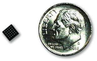
▲그림 1 : LTM8074는 사일런트 스위처(Silent Switcherⓡ) 아키텍처를 적용해서 매우 작은 패키지로 완전한 저잡음 솔루션을 제공한다.
EN 55022 Class B 같은 대부분의 EMI 적합성 요건을 충족하는 보다 정숙한 DC-DC 변환과 작은 풋프린트 외에도, PCB 상에서 출력 커패시터 같은 외부 부품 수를 최소화한다는 점 또한 중요하다.
DC-DC 레귤레이터가 과도 응답이 빠르면 출력 커패시턴스에 대한 의존도를 낮출 수 있다.
이는 최적화된 내부 피드백 루프 보상 덕분에 설계가 간소해지고, 이로써 광범위한 동작 조건에서 다양한 종류의 출력 커패시터를 사용해서 충분한 안정성 마진을 제공한다는 것을 의미한다.
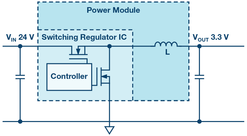
▲그림 2 : 스텝다운(벅) 스위칭 레귤레이터가 인덕터와 함께 전원 모듈에 통합되어 있다.

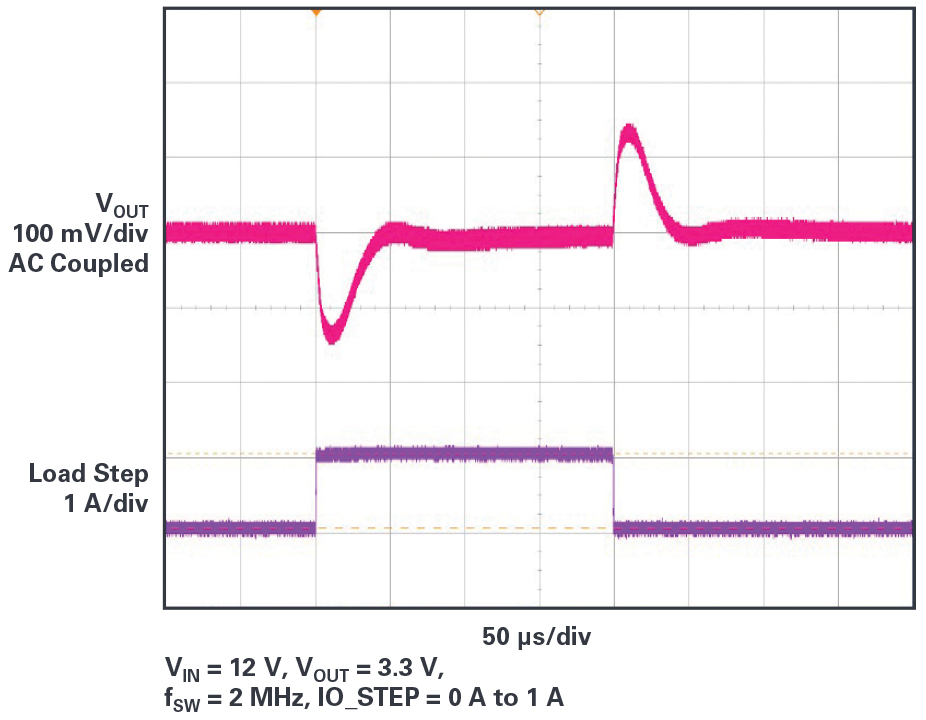
▲그림 3 : LTM8074는 최소한의 출력 커패시터(2 x 4.7 F 세라믹)를 사용해서 빠른 과도 응답을 달성한다(12VIN, 3.3VOUT).
LTM8074는 1.2A 40VIN 마이크로모듈(μModule) 스텝다운 레귤레이터로서, 극히 소형화된 4㎜ x 4㎜ x 1.82㎜ 크기와 0.65㎜ 피치의 BGA 패키지이다. 전체적인 솔루션 크기는 3.2VIN∼40VIN, 3.3VOUT일 때 60㎟이며, 2개의 0805 커패시터와 2개의 0603 저항만을 필요로 한다.
또한 패키지 높이가 낮고 무게가 가벼우므로(0.08그램), PCB 상단면에 다른 부품들이 빽빽하게 탑재되었을 때 이 디바이스를 PCB 하단면에 탑재할 수 있다. 또한 LTM8074는 사일런트 스위처 아키텍처를 적용해서 EMI 방사를 최소화하므로 CISPR22 Class B 요건을 여유 있게 충족하고, 다른 민감한 회로들에 대한 EMC 취약성을 낮출 수 있다.
모든 외부 소자들을 통합한다는 것은 불가능하다. 이유는 간단하다. 예를 들어 스위칭 주파수나 소프트 스타트 시간 같은 설정을 조절 가능하게 하려면 회로에게 어떻게 하라고 말해주는 것이 필요하다.
이것은 디지털 방식으로 할 수 있다. 그러려면 마이크로컨트롤러와 비휘발성 메모리를 사용해야 한다는 뜻인데, 이는 시스템 비용 증가로 이어진다.
이를 피하기 위해서 흔히 사용하는 방법이 외부 수동 부품들을 사용해서 이러한 설정을 할 수 있도록 하는 것이다.
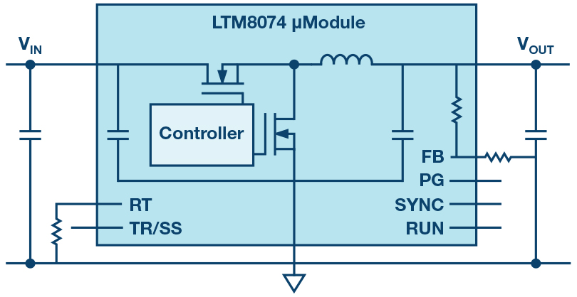
흔히 입력과 출력 커패시터를 전원 모듈 안에 통합하는데, 때로는 외부에 필요할 수도 있다. 그림 4는 아나로그디바이스(Analog Devices)의 LTM8074를 사용한 회로를 보여준다.
▲그림 4 : LTM8074는 불과 4㎜ x 4㎜ 크기로 최대 40V VIN 및 1.2A 출력 전류를 제공한다.
하나의 외부 저항만을 사용해서 원하는 출력 전압을 설정할 수 있으므로 제품의 모델 유형을 줄일 수 있고, 애플리케이션에 어느 정도의 유연성도 제공한다. 소프트-스타트 기능이 필요하지 않을 때는 해당 핀에 커패시터를 연결할 필요가 없다. 이 모든 특징들은 극히 소형화된 보드 면적에서 전압 변환을 구현할 수 있게 해준다.
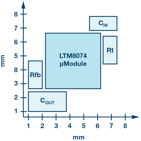
LTM8074는 크기가 4㎜ x 4㎜에 불과하고 최소한의 외부 배선만을 필요로 하므로, 약 8㎜ x 8㎜에 불과한 보드 면적에서 최대 40V 입력 전압과 최대 1.2A까지 허용 가능한 출력 전류를 지원하는 완전한 전원공급장치를 구현할 수 있다. 그림 5는 최소한의 외부 부품만을 사용한 레이아웃의 결과이다.
▲그림 5 : 보드 면적이 약 8㎜ x 8㎜인 레이아웃 예시
작은 전원공급장치의 경우는 매우 높은 변환 효율이 매우 중요하다. 그렇지 않으면 열 발산과 관련해서 문제가 있을 수 있다.
이 점에 있어서도 새로운 초소형 LTM8074는 이상적인 선택이다. 사일런트 스위처 기술을 적용한 덕분에, 이 제품은 잡음에 특히 민감한 회로에 사용하기에 적합하다. 통상적으로는 이러한 회로에 선형 레귤레이터를 주로 사용한다.
고도로 통합된 전원 모듈은 SMPS 설계를 간소화할 뿐 아니라, 굉장히 작은 공간에서 효율적인 전압 변환을 달성하기 위해서도 적합하다.
ADI Module 디바이스의 성능 특징은 다음과 같이 요약할 수 있다.
- 더욱 낮은 잡음(초저 잡음 및 사일런트 스위처 디바이스)
- 초박형 패키지
- 6면에 걸친 효율적인 냉각(CoP)
- 라인, 부하, 온도에 대해서 정밀한 VOUT 레귤레이션
- 극한의 신뢰성 테스트
- 접지 루프 최소화
- 다중 출력 제공 가능
- 극한의 온도 테스트
※ 저자 소개
프레드릭 도스탈(Frederik Dostal) FAE / 아나로그디바이스(Analog Devices, Inc.)
프레데릭 도스탈(Frederik Dostal)은 독일 뉘른베르크에 있는 에를랑겐 대학에서 마이크로일렉트로닉스를 전공했다. 2001년에 전원 관리 분야에서 경력을 시작했으며, 애리조나주 피닉스에서 4년 간 스위치 모드 전원공급장치(SMPS)와 관련한 업무를 맡은 것을 비롯해 다양한 애플리케이션 직책을 거쳤다. 아나로그디바이스(Analog Devices)에는 2009년에 입사했으며, 현재는 ADI 뮌헨 지사에서 전원관리 FAE로 재직 중이다.

Comments
Related news

[Technical Contribution] ADI Frederic Dostal - How to Miniaturize Power Supplies
Analog Devices' Frederik Dostal discusses the miniaturization of power supply units.
2022.07.12by 명세환 기자

[Technical Contribution] ADI Frederic Dostal – Dynamic Control Method for Optimal Output Voltage
Let's hear from Frederik Dostal, FAE at Analog Devices, Inc., about the dynamic adjustment method for appropriate output voltage.
2022.12.06by 명세환 기자

[Technical Contribution] ADI's Frederik Dostal: Designing More Compact Power Supplies with Just One Inductor
We spoke with Frederick Dostal of ADI about methods for designing more compact power supplies using just a single inductor.
2023.03.14by 명세환 기자

Intel Unveils Next-Generation 'Core Ultra Series 3' and vPro Platform for Enterprise PCs
Intel has officially unveiled the "Intel Core Ultra Series 3" for next-generation enterprise PCs and the latest vPro platform, addressing a wide range of demands from enterprise notebooks to high-performance workstations.
2026.03.26by 배종인 기자

ROHM Launches ESD Protection Diode Compatible with High-Speed Interfaces of 10Gbps or Higher
Semiconductor specialist ROHM has developed the 'RESDxVx series' of ESD (electrostatic discharge) protection diodes capable of responding to next-generation high-speed data communication environments exceeding 10Gbps, simultaneously enhancing both signal quality maintenance required in high-speed interfaces and IC protection performance.
2026.03.26by 배종인 기자











