



ADI Invests Over $1 Billion to Expand Oregon Semiconductor Fab Facilities
 Published2023.07.28 12:23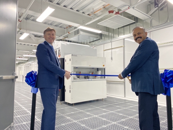
Analog Devices (ADI) is expanding its semiconductor fab facility in Oregon, and ADI's own production volume manufactured at advanced micro-process nodes is expected to nearly double.
ADI announced on the 28th that it is investing more than $1 billion to expand its semiconductor wafer fab facility in Beaverton, Oregon.
Completed in 1978, the Beaverton Fab is ADI's largest wafer manufacturing facility by production volume and serves customers in key industrial sectors such as industrial, automotive, telecommunications, consumer electronics, and healthcare.
With this facility investment, the cleanroom space will increase to approximately 118,000 square feet (about 11,000 square meters), and ADI's in-house production capacity for manufacturing at advanced micro-process nodes of 180 nanometers or more will nearly double.
Along with this, by creating hundreds of new long-term jobs, the number of ADI employees working in Oregon is expected to increase significantly from the current approximately 950.
More than 10% of the total investment is used to purchase the latest advanced fab equipment to increase overall efficiency and utilize more environmentally friendly chemicals. This facility aims to nearly double production while reducing absolute greenhouse gas emissions by about 75% and water usage per unit of production by about 50%.
Vincent Roche, CEO and Chairman of ADI, said, “By expanding the Beaverton fab facility, ADI will increase production capacity in key industrial sectors, boost domestic manufacturing in line with the spirit of the Semiconductor Support Act (CHIPS Act), and strengthen the global resilience of ADI’s hybrid manufacturing model, which utilizes both in-house fabs and external foundries. Our investment in Beaverton will facilitate the achievement of these goals through the incredible dedication and talent of ADI’s existing workforce and the leverage of Oregon’s strong talent pool.”
U.S. Senator Ron Wyden of Oregon said, “Analog Devices’ investment announcement is a significant step forward in ensuring that Oregon fully benefits from the federal CHIPS Act, which I worked to pass. This announcement will strengthen Oregon’s flagship industry by solidifying the semiconductor industry’s position in Silicon Forest and the surrounding area, creating quality new jobs in Beaverton to exert influence at the state level, and providing a boost to the Oregon economy as a whole.”
The Semiconductor Advanced Manufacturing University (SAMU), a talent development training center that provides an 8-week course of training for groups of approximately 25 students each regarding semiconductor equipment maintenance, is scheduled to be established at the ADI Beaverton facility. Through this training center, ADI plans to provide educational opportunities for a curriculum focused on basic semiconductor manufacturing training and advanced professional development to diverse groups in the local community, including U.S. military veterans, job seekers, and existing ADI factory workers.
ADI's hybrid manufacturing model is an extensive network consisting of in-house factories and external partners. This model enables ADI to effectively manage operations according to economic cycles, strengthen the resilience of its global supply chain, and better respond to customer demand. To improve operations at its in-house fabs, ADI increased capital investment from 4% of past revenue through fiscal years 2022 and 2023 to a high single-digit percentage. These investments are taking place across ADI's global manufacturing facilities, including those in Washington and Massachusetts in the U.S., as well as in Ireland, Thailand, Malaysia, and the Philippines.

Comments
Related news

Intel Unveils Next-Generation 'Core Ultra Series 3' and vPro Platform for Enterprise PCs
Intel has officially unveiled the "Intel Core Ultra Series 3" for next-generation enterprise PCs and the latest vPro platform, addressing a wide range of demands from enterprise notebooks to high-performance workstations.
2026.03.26by 배종인 기자

ROHM Launches ESD Protection Diode Compatible with High-Speed Interfaces of 10Gbps or Higher
Semiconductor specialist ROHM has developed the 'RESDxVx series' of ESD (electrostatic discharge) protection diodes capable of responding to next-generation high-speed data communication environments exceeding 10Gbps, simultaneously enhancing both signal quality maintenance required in high-speed interfaces and IC protection performance.
2026.03.26by 배종인 기자

ST Launches 75V Drive IC Targeting 48V Industrial Motor Driving
ST Microelectronics has unveiled the 'STSPIN9P' series of 75V motor drive ICs tailored for 48V-class industrial drive system design. The new product family is characterized by half-bridge and full-bridge configurations that enable design scalability according to motor type and output conditions. Power supply circuits, protection functions, and current sensing circuits are integrated on-chip to simplify system configuration, and the devices are designed to support applications up to 500W maximum. The company plans to provide reference designs and demo boards to support development and evaluation in industrial automation, robotics, pumps, fans, lighting, and textile machinery.
2026.03.26by 배종인 기자

Nordic supports security updates for the entire lifecycle of IoT devices at a single fixed cost
Nordic Semiconductor, a global leader in low-power wireless connectivity solutions, has unveiled a single fixed-cost licensing model that delivers FOTA (Firmware Over-the-Air) and device management capabilities throughout the device lifecycle via nRF Cloud, and introduced a new firmware update solution to prepare for the enforcement of the European Union's Cyber Resilience Act (CRA).
2026.03.26by 배종인 기자

Practical Training in Low-Noise, Low-Power Circuit Design All in One Place… Training Fee Support
The "2026 Advanced Engineer Practical Masterclass" to strengthen competencies in high-sensitivity analog circuit and sensor-based system design will be held on April 16 at the e4ds Conference Center in Gasan-dong, Seoul. This program will be conducted as an offline paid hands-on training session, not online, and is targeted at engineers seeking on-site intensive learning. Texas Instruments will provide educational support for this training, allowing participation at 150,000 won, a 100,000 won discount from the original price of 250,000 won.
2026.03.26by 배종인 기자











