


ETRI develops light source element to solve data explosion
 Published2024.01.26 14:16
.jpg)
▲ETRI researchers demonstrating the transmission characteristics of a field-absorbing light source device
Double the modulation bandwidth and data processing capacity per channel compared to before
A domestic research team has developed the world's first optical source element that can be used in ultra-large data centers and 5G/6G mobile communication base stations. The researchers' technology can transmit 5.6 5GB full HD movies per second.
The Electronics and Telecommunications Research Institute (ETRI) announced on the 24th that it has successfully developed an electro-absorption modulation type optical source element technology smaller than a millimeter (mm) in size (0.2mm x 0.85mm) that can transmit 224Gbps optical signals per channel for use in the internal networks of data centers.
The research team developed an electro-absorption modulation type light source device with a single integrated optical mode converter and monitoring photodetector using domestic technology from design to manufacturing.
The light source device that the research team successfully developed will be installed in tower racks inside large-scale data centers when commercialized in the future.
The light source element goes into the transmitter section of the optical transceiver (optical transmission/reception module).
The optical transceiver is connected to a line card inside the tower rack.
Typically, 32 224-gigabit (G) 8-channel optical transceivers constitute one line card, and multiple line cards are mounted in a tower rack.
The research team has shifted away from the previous focus on module development and placed greater importance on the development of chip units, which are core source technologies.
He explained that because they have developed the core technology of the light source chip, they will be able to lead the global optical communications market in the future.
Recently, with the increase in data usage such as virtual reality (VR), augmented reality (AR), OTT, and artificial intelligence, there is a need for an ultra-high-speed optical source technology for transmission within data centers that enables implementation of low-cost optical modules with larger modulation bandwidth and data processing capacity.
For optical transceivers used inside existing data centers, an electro-absorption modulation type optical source element capable of transmitting optical signals of up to 100 Gbps per channel is used.
ETRI has developed the world's best electro-absorption modulation type optical source element capable of transmitting 224 Gbps optical signals per channel by doubling the modulation bandwidth and data processing capacity..
In addition, an optical mode converter that can increase optical coupling efficiency and a photodetector that can monitor the optical output intensity of the light source element in real time were integrated into a 224 Gbps electro-absorptive modulation light source element for the first time in the world.
By integrating the optical mode converter, the optical coupling efficiency has been significantly improved, increasing the coupling efficiency with the optical waveguide from the previous 50% to 85%, thereby reducing energy consumption.
In addition, through the single integration of a photodetector that monitors the optical output intensity, the packaging cost can be significantly reduced in the production of single-channel optical modules as well as 800G/1.6Tbps-class optical modules compared to the existing structure using a separate photodetector.
The 224Gbps electro-absorption modulation light source device developed by the research team this time showed a modulation bandwidth of over 70GHz at 70℃, which is the world's highest level.
This is an excellent performance that enables 224 Gbps, 2 km optical transmission not only at room temperature but also at 70℃.
The research team explained that the 224Gbps-class electro-absorption modulation light source device is currently being developed by only a few companies worldwide, and that the development of this technology will allow for the elimination of dependence on overseas imports in the future.
In addition, since the optical mode converter and monitoring photodetector are integrated into a single device, it is expected to contribute to the price competitiveness of the 800G/1.6Tbps optical module along with its technological competitiveness.
ETRI stated that this research result was possible because the research team possessed core compound semiconductor technology, such as laser diode technology for making light sources and core compound semiconductor technology that they have accumulated leading the way in R&D foundries.
ETRI Baek Yong-sun, head of the Stereoscopic Communication Research Lab, said, “We have been able to contribute to securing the competitiveness of the domestic optical device and parts industry by developing core technologies that can be applied to the rapidly growing data center and 5G/6G markets for the first time in the world.”Did.
ETRI Optical Communication Components Research Lab Senior Researcher Han Yeong-tak also said, “In the case of compound optical semiconductors, which are very sensitive to process variables, securing core source technologies and stable foundry operation are the most important issues, and we have solved this problem by developing core technologies.”
The research team applied for domestic and international patents using the developed light source technology.
We plan to transfer technology to domestic optical component companies to help them compete with global companies in the data center and 5G/6G markets.
According to market research firm Light Counting, the global optical transceiver market size is expected to grow more than threefold from $6 billion in 2019 to $18 billion in 2026.
Meanwhile, the ETRI research team announced this technology at OFC 2023, the world's largest optical communications conference held in San Diego, USA in March of last year.
The technical prowess was greatly recognized by being published in the IEEE JLT international SCI paper.
This achievement was made possible through the Ministry of Science and ICT's 'Development of optical component technology for 1.6Tbps optical transceiver for intra-DC communication' project.

Comments
Related news
ETRI Achieves World-Leading 3Gbps 5G Small Cell Speed
The Electronics and Telecommunications Research Institute (ETRI) has successfully developed dual connectivity technology that simultaneously utilizes Sub-6GHz (mid-band) and millimeter wave (mmWave, high-band) frequencies as part of the '5G NR-based Intelligent Open Small Cell Technology Development' project, a broadcasting and telecommunications industry technology development initiative funded by the Ministry of Science and ICT.
2023.12.19by 배종인 기자
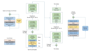
MediaZen and ETRI Develop Voice Recognition System 40% Faster Than Google
A speech recognition system with a convolutional network architecture featuring 40% improved processing speed has been developed to provide a latency-free speech recognition solution.
2023.12.26by 명세환 기자

ETRI Performs Robotic Tasks Without Programming
The Electronics and Telecommunications Research Institute (ETRI) announced on the 27th that it has developed a technology that enables complex tasks requiring control of speed, acceleration, and contact force using a robotic arm without requiring professional programming education.
2023.12.28by 김예지 기자

ETRI, 2024 Research and Management Vision: 'Securing Strategic and Core Technologies'
The Korea Electronics and Telecommunications Research Institute announced its research and management vision for the year alongside a New Year's address. Additionally, representative research achievements and award-winning technologies that distinguished 2023 were unveiled.
2024.01.03by 명세환 기자
.jpg)
ETRI, Game Analysis AI Development… “LoL Win Rate Prediction Accuracy 87%”
The Electronics and Telecommunications Research Institute (ETRI) announced on the 5th that it has developed a technology that analyzes play elements extracted from game footage to recognize real-time game situations in progress, detects major in-game play events, and automatically generates highlights. This technology was applied to the game 'League of Legends (LoL)' at a recently held international esports tournament and received positive response.
2024.01.05by 김예지 기자











