



Ministry of Science and ICT Hosts 'My Chip' Talk Concert
 Published2024.02.15 15:11
Sharing my experience participating in the My Chip lecture in the semiconductor design field
Semiconductor majors visit the Korea Electronics and Telecommunications Research Institute public fabrication plant
With the demand for high-tech talent continuing to rise and corporate needs for practical skills growing, a meeting was held to share experiences and discuss activation strategies for the 'My Chip Service,' which aims to enhance the capabilities of university students in the semiconductor design field.
The Ministry of Science and ICT held a 'My Chip Talk Concert' with semiconductor majors at the Korea Electronics and Telecommunications Research Institute in Daejeon on the 15th.
Semiconductor design experts from the field and students participating in the My Chip service discussed ways to strengthen semiconductor design capabilities and foster talent.
The My Chip service, which fosters design talent with practical capabilities by providing undergraduates—who previously could only use design software—with the opportunity to manufacture their own designed chips, is planned to be continuously expanded.
My Chip Service is a project supported by the Ministry of Science and ICT since last year, in which semiconductor chips designed by students are manufactured and packaged at 500nm CMOS (Complementary Metal-Oxide Semiconductor) fabs operated by the Electronics and Telecommunications Research Institute, Seoul National University, and Daegu Gyeongbuk Institute of Science and Technology, and then provided to the students.
Through this, students can use the chip they designed.It is expected that one can grow into a semiconductor design expert by actually verifying whether it operates as intended and performing measurements and analyses.
At this talk concert, Park Sung-hyun, CEO of Rebellion and an expert in semiconductor design, and Kim Hye-ji, a senior researcher at the Electronics and Telecommunications Research Institute, participated to communicate with students studying semiconductor design about undergraduate and graduate life, stories of employment and entrepreneurship, life as a semiconductor design expert, and recent technology trends.
In addition, Lee Dong-young from Kyung Hee University and Lee Seung-hyun from Chung-Ang University, who participated in the first My Chip service, shared their experiences and insights from the My Chip design project, conveying stories from the field and discussing ways to revitalize the related service.
Currently, the My Chip service plans to accept applications for a total of four times, once per quarter, through the 'My Chip website (mpw.kion.or.kr)', and applications for the first service are being accepted until February 29.
In addition, participating students can communicate with each other through the online community newly opened on the My Chip website in February, and a student exchange event is also planned for the second half of the year.
Minister Lee Jong-ho of the Ministry of Science and ICT said, “This talk concert was a valuable opportunity for students participating in the My Chip service to envision their future as design experts through meetings with semiconductor design experts, and to discuss in depth the significance of the My Chip service in the educational field.”
In addition, he stated, “We will do our best to create an innovative educational environment so that more students can become excellent semiconductor design experts by expanding the scale of My Chip service support sixfold compared to last year and activating exchanges among participating students.”
Meanwhile, last January, the Ministry of Science and ICT, together with the Ministry of Trade, Industry and Energy, held three events under the theme of 'The Semiconductor Industry Enriching People's Livelihoods'At the public livelihood forum held with the people, the 'Plan for the Creation of a Semiconductor Mega Cluster' was announced, which includes four key tasks for building a semiconductor mega cluster: infrastructure and investment environment, ecosystem, cutting-edge technology, and talent.

Comments
Related news
The Ministry of Science and ICT stated, "The number of 5G locations nationwide doubled to 54 last year."
The Ministry of Science and Technology Information and Communication announced on the 3rd that usage of the 5G Network has increased more than twofold compared to the previous year, expanding to 54 locations across 30 companies and organizations nationwide as of the end of 2023.
2024.01.03by 김예지 기자
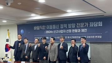
“5G 28GHz 4th Mobile Communication Support Policy Must Be Transparent”
Some experts have expressed skepticism regarding the discovery of new 5G 28GHz operators being pursued under the Ministry of Science and ICT's telecommunications market competition promotion initiative. While there are expectations that activation of the 28GHz business, which the three major telecom carriers have abandoned, can be achieved, the necessity for establishing safeguards to address concerns about the feasibility of achieving the original objectives of telecommunications market competition promotion is emerging.
2024.01.17by 김예지 기자
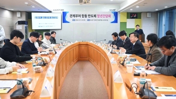
The last piece of the semiconductor cluster puzzle, the 'talent development' team
The relevant ministries, including the Ministry of Industry, Energy and Resources, the Ministry of Education, and the Ministry of Science and ICT, will work as one team to accelerate semiconductor future talent development, which is a key initiative and critical factor for success in the 'Semiconductor Mega Cluster Formation Plan' announced on the 15th.
2024.01.26by 권신혁 기자

Ministry of Science and ICT to Promote 6G·OpenLAN Talent Development Project worth 60 Billion Won
As the paradigm of network technology and industry shifts toward cloud (virtualization) and OpenRAN (openization) technology-centric approaches, the Ministry of Science and Technology is promoting a global talent development project for 6G and OpenRAN to maintain leadership in next-generation network technology.
2024.02.06by 김예지 기자
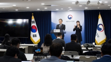
Repeal the Single-Targeting Act and Activate On-Device AI
The Ministry of Science and Technology announced its major policy promotion plans for 2024 on the 13th, targeting a leap forward as a global science and technology powerhouse and a digital model nation. The ministry stated it will abolish the Mobile Device Distribution Act and expand the launch of mid-to-low-priced terminals as a digital-based livelihood stabilization policy.
2024.02.14by 김예지 기자











