


[Technical Contribution] ADI Develops Scalable Beamforming Engine for Quad-Apollo MxFE Radar and Communications Systems
 Published2026.01.12 11:10
1도 이하 위상 정렬·피코초 수준 타이밍 정확도 달성 시스템 검증
■ 쿼드-아폴로 MxFE™ X-밴드 디지털 빔포밍 플랫폼의 설계·구현
이 글에서는 아나로그디바이스(Analog Devices)의 아폴로(Apollo) MxFE™(mixed-signal front end) 기술이 제공하는 모든 성능을 입증하기 위해 개발된 첨단 직접 RF 샘플링 레퍼런스 아키텍처인 쿼드-아폴로 MxFE™ X-밴드 디지털 빔포밍 플랫폼의 설계와 구현을 소개한다.
이 플랫폼은 동기화된 클러킹, 결정론적 트리거링, 위상 코히어런트(phase-coherent) 타이밍을 갖춘 4개의 트랜시버를 통합해 X-밴드 주파수에서 각각 16개씩의 송신 및 수신 채널에 대해 진정한 디지털 빔포밍을 구현한다.
이는 저잡음 RF 프런트엔드, 정밀 클럭 생성, 멀티칩 동기화, 전원 분배를 포함한 포괄적인 신호 체인을 구현함으로써 광대역 동작과 멀티빔 지원이 가능한 확장형 위상 코히어런트 어레이를 실현했다.
■ 차세대 디지털 빔포밍 시스템 위한 완전한 레퍼런스 아키텍처 제공
쿼드-아폴로(Quad-Apollo) MxFE™ X-밴드 직접 샘플링 디지털 빔포밍 플랫폼(그림 1)은 모든 소자에 디지털 직접 RF 샘플링을 적용한 첨단 솔루션으로서, 차세대 디지털 빔포밍 시스템을 위한 완전한 레퍼런스 아키텍처를 제공한다.
아나로그디바이스(Analog Devices)의 MxFE® 기술 역량을 부각하도록 설계된 이 플랫폼은 RF 신호 컨디셔닝, 정밀 클러킹, 멀티칩 동기화, DC 전원 관리 등 모든 핵심 서브시스템을 하나의 고성능 환경으로 통합해, 여러 채널에 걸쳐 위상 코히어런트성과 확장 가능한 신호 처리를 지원한다.
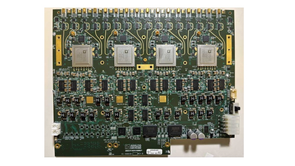
플랫폼 내 각 서브어레이는 균일한 리니어 어레이로 구성된 각각 16개씩의 수신 및 송신 채널로 이루어져 있으며, 소자 간 간격은 12GHz에서 반파장에 해당하도록 설계되었다.
이러한 배열 구조는 X-밴드 동작에 최적화된 공간 샘플링을 가능하게 하는 동시에, 모든 소자에 대해 완전한 디지털 빔포밍을 지원한다.
또한 이 플랫폼은 다수의 AD9084 아폴로 MxFE 데이터 컨버터를 하나의 위상 코히어런트 아키텍처 내에서 원활하게 동기화하고 클러킹할 수 있음을 보여주며, 다채널 RF 애플리케이션을 위한 시스템 레벨 통합의 현실적인 사례를 제시한다.
쿼드-아폴로 MxFE 플랫폼은 레퍼런스 디자인으로서의 역할을 넘어, 첨단 레이더 및 통신 시스템을 위한 범용 개발·평가 도구로 활용될 수 있다.
이 아키텍처는 여러 개의 동시 빔, 적응형 널링(adaptive nulling), 재구성 가능한 빔 패턴을 지원해, 최신 위상 배열 레이더, 전자전(EW), 다중 임무 센싱 애플리케이션에서 요구하는 유연성을 제공한다.
이 시스템의 결정론적 타이밍 프레임워크, 광대역 프런트엔드, 확장형 동기화 구조는 RF 입력에서부터 디지털 빔포밍 출력에 이르는 완전한 신호 체인을 구현함으로써, 고속 모든 소자 디지털 배열 기술의 혁신을 가속화하도록 설계되었다.
그림 2의 블록 다이어그램은 단일 서브어레이의 송신 및 수신 RF 프런트엔드 신호 체인, 강화된 디지털 신호 처리 기능을 탑재한 데이터 컨버터, 멀티칩 클러킹 솔루션, 그리고 12V DC 전원 솔루션을 보여준다.
이 솔루션은 상용 기성품(COTS) FPGA 캐리어 카드와 낮은 수준의 오픈소스 소프트웨어 드라이버 및 MATLAB® 툴박스를 결합하고 있어 시스템 플랫폼에 대한 소프트웨어 제어가 가능하다.
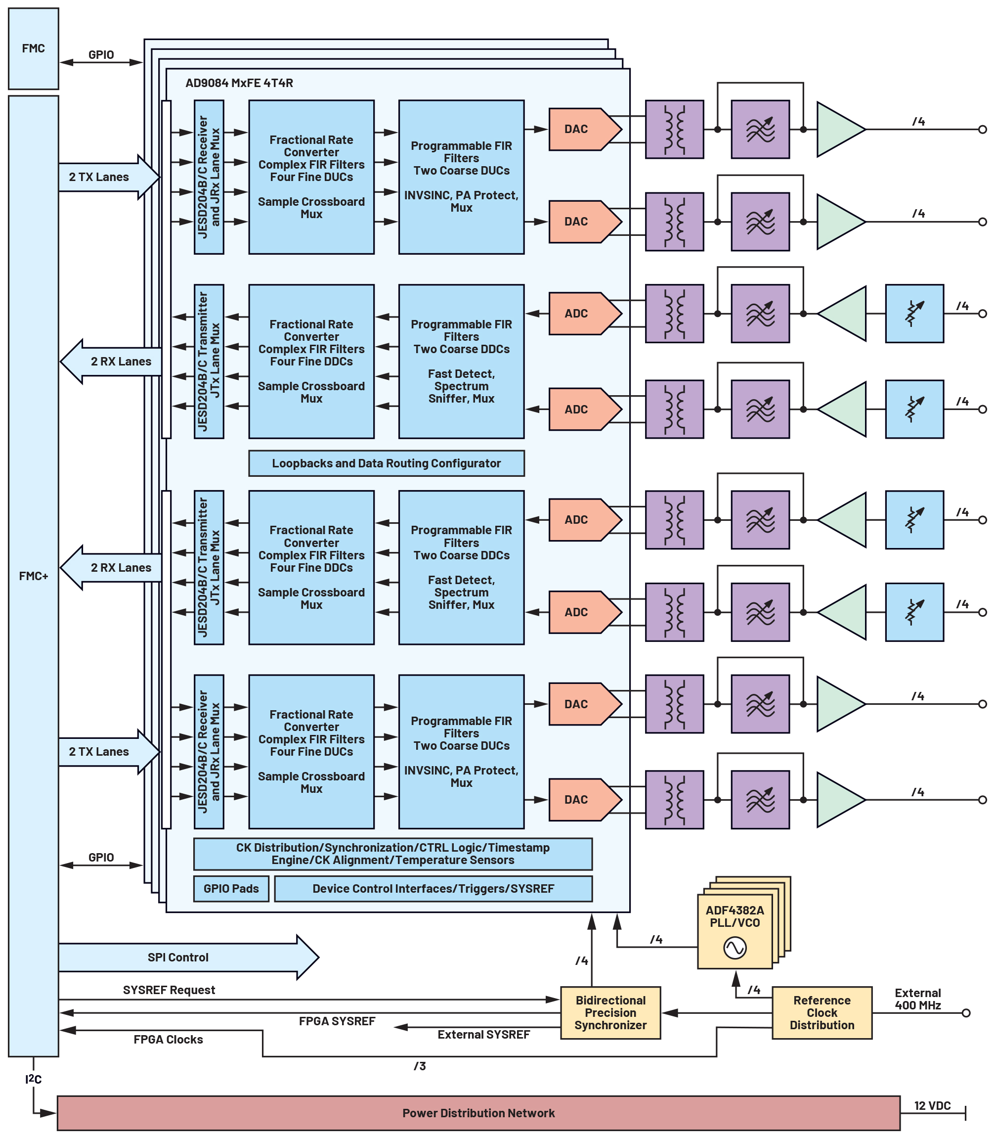
▲그림 2. ADF4382A를 포함한 쿼드-아폴로 MxFE 전체 시스템 블록 다이어그램

■ RF 프런트엔드
쿼드-아폴로 MxFE 시스템의 RF 프런트엔드는 의도적으로 단순성과 모듈성을 강조한 구조로 설계되어, 다양한 애플리케이션에 높은 유연성과 성능, 그리고 손쉬운 맞춤화 특성을 제공한다.
그림 3과 그림 4에 나타난 바와 같이, 이 아키텍처는 광대역이면서도 그리 복잡하지 않은 신호 경로를 활용해 넓은 주파수 커버리지를 확보하는 동시에, 전체 신호 체인에 걸쳐 높은 선형성과 신호 무결성을 유지하도록 한다.
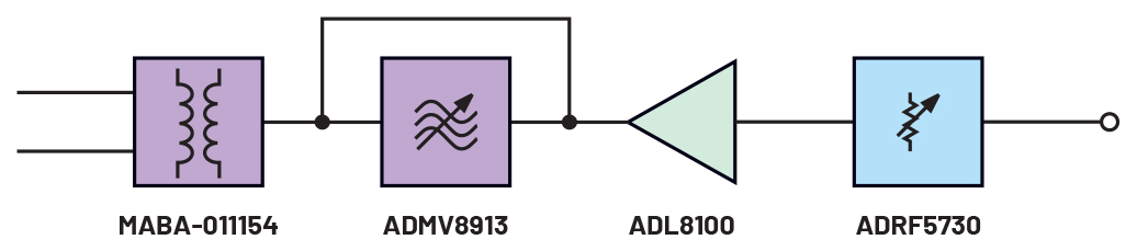
▲그림 3. ADMV8913, ADL8100, ADRF5730을 포함하는 수신기 신호 체인 블록 다이어그램
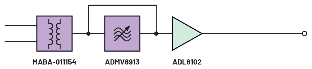
이 시스템은 고속 ADC 및 DAC를 아날로그 신호 체인의 나머지 부분과 연결하기 위해 2:1 광대역 발룬(balun)을 채택하고 있는 것이 설계의 핵심적인 특징 중 하나이다.
각 송수신 채널에는 디지털 방식으로 튜닝 가능한 X-밴드 필터 ADMV8913이 공용으로 통합되어 있으며, 이를 통해 정밀한 주파수 선택과 대역 외(out-of-band) 신호 배제를 구현한다.
이 필터단에는 커패시터 회전 메커니즘을 통해 활성화할 수 있는 보드 레벨 바이패스 경로가 포함되어 있어 S-밴드, C-밴드, Ku-밴드 주파수에서 직접 샘플링이 가능하다.
필터를 바이패스할 경우 ADMV8913이 제공하는 고유한 안티앨리어싱 이점은 줄어들지만, 디지털 방식으로 필터링을 처리할 수 있는 광대역 또는 와이드밴드 애플리케이션에서는 더욱 확장된 주파수 유연성을 확보할 수 있다.
수신 경로에서, 각 채널은 비교적 단순하지만 매우 높은 선형성을 갖춘 광대역 저잡음 증폭기(LNA)와, 입력단에 배치된 광대역 디지털 스텝 감쇠기(DSA)로 구성된다.
DSA는 다양한 신호 조건에 걸쳐 세밀한 아날로그 이득 제어를 가능하게 하며, 시스템 동작 중에도 빠르고 결정론적인 조정이 가능하도록 데이터 컨버터의 GPIO 인터페이스를 통해 직접 제어된다.
이 아키텍처는 신속한 재설정을 지원해, 적응형 또는 실시간 빔포밍 시스템에 특히 적합하다.
수신기의 선형성은 이 설계에서 특별히 강조된 부분이다.
완전 디지털, 모든 소자의 위상 배열 시스템에서는 상호변조 왜곡 성분이 소자들 간에 공간적으로 상관되는 경향이 있기 때문이다.
선형성을 우선적으로 확보함으로써, 쿼드-아폴로 MxFE 기술은 다채널 위상 코히어런트 구성에서도 동적 범위와 스펙트럼 순도를 안정적으로 유지한다.
추가적인 주파수 변환, 이득 단계, 또는 특수한 신호 컨디셔닝이 필요한 애플리케이션을 위해, 이 플랫폼은 프런트엔드 앞단에 플러그인 형태의 퍼스낼리티 카드를 통합할 수 있도록 지원한다.
이러한 모듈형 확장 기능을 통해 시스템 설계자는 대역폭, 잡음 지수, 주파수 커버리지 등 특정한 최종 용도 요구사항에 맞춰 성능 범위를 유연하게 조정할 수 있다.
서브어레이 레벨의 신호 체인을 간결하고 광대역으로 유지함으로써, 쿼드-아폴로 MxFE 시스템은 확장 가능한 고성능 RF 시스템 개발을 위해 강건하면서도 유연한 기반을 제공한다.
■ 클러킹 아키텍처
클러킹은 오늘날의 멀티 컨버터 시스템에서 핵심적인 역할을 수행하며, 멀티칩 동기화, 균일한 지연, 그리고 대규모 분산형 아키텍처 전반에 걸친 위상 코히어런트 신호 결합을 가능하게 하는 근간이 된다.
정밀한 클럭 분배는 모든 데이터 컨버터, FPGA, 아날로그 프런트엔드가 완벽한 조화를 이루며 동작하도록 보장하는데, 이는 위상 배열 레이더, 다채널 계측 시스템, 첨단 통신 시스템과 같은 애플리케이션에서 필수적으로 요구되는 사항이다.
이러한 시스템에서 JESD204C 표준 기반의 동기화는 전용 클럭 생성 블록과 클럭 분배 블록의 조합, 그리고 양방향 서브클래스 1 동기화기를 통해 구현된다.
이 아키텍처는 모든 JESD204C 채널 전반에 걸쳐 균일한 지연을 보장함으로써, 시스템 설계자가 나노초 수준의 정밀도로 타이밍을 예측 및 제어할 수 있도록 한다.
또한 이 동기화 구조는 단일 서브시스템 이상으로 확장이 가능해, 대규모로 구현되어야 하는 애플리케이션에서도 여러 서브어레이 간에 지연을 균일하게 유지할 수 있다.
그림 5에 보이는 것처럼, 안정성이 높은 단일 기준 클럭이 전체 타이밍 네트워크의 기반을 이룬다.
이 기준 신호는 지터가 극히 낮은 클럭 팬아웃 버퍼를 통해 분배되어, MxFE 디바이스에 매우 깨끗한 초저 위상 잡음의 샘플링 클럭을 공급한다.
각 MxFE 디바이스는 전용 2선식 클럭 인터페이스를 사용해 위상과 주파수 정렬을 지속적으로 유지하며, 온도 변화나 장기 운용으로(long-term aging) 인해 발생하는 드리프트를 보상한다.
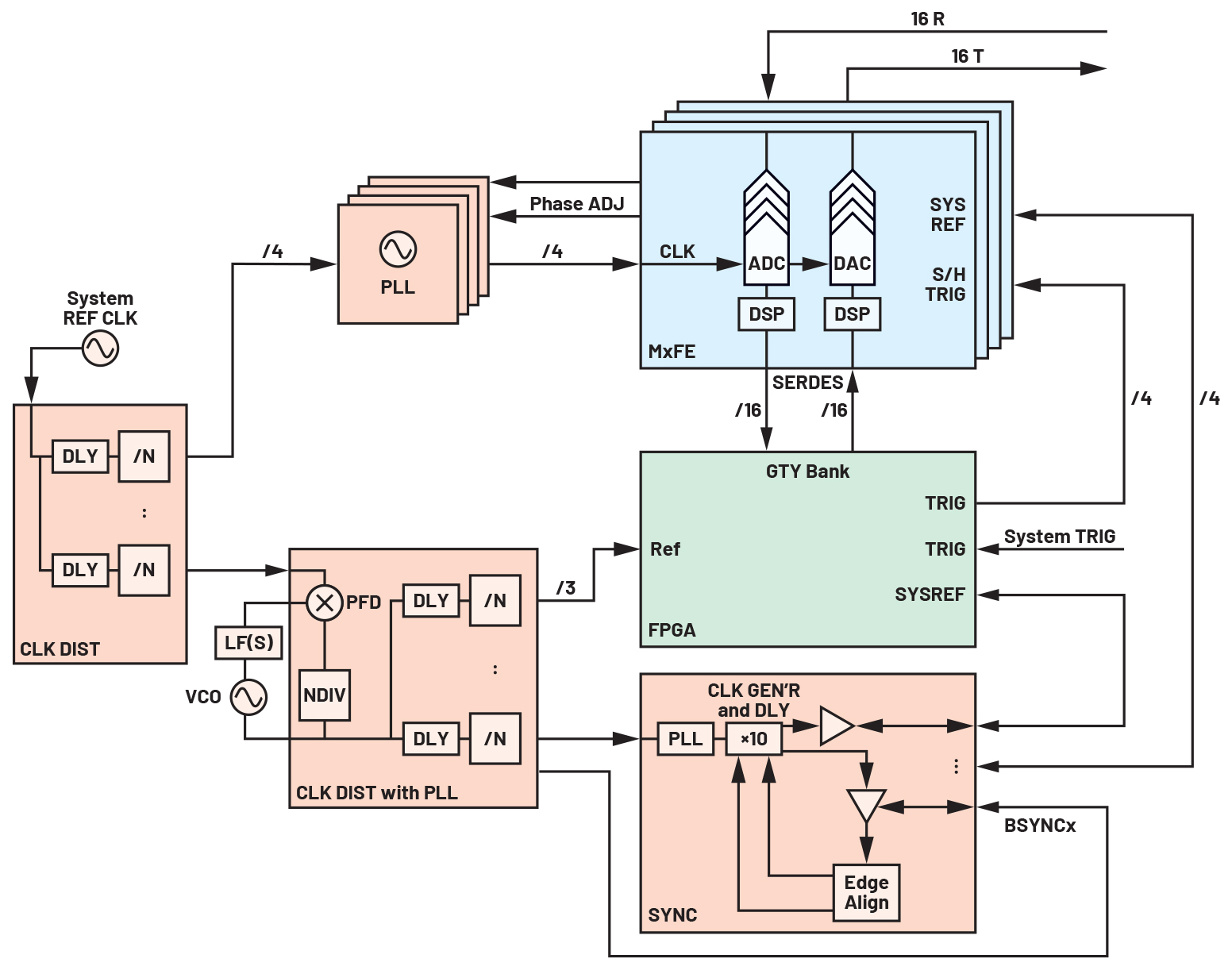
▲그림 5. 클러킹 아키텍처 블록 다이어그램
동일한 마스터 기준 클럭은 FPGA 패브릭을 위한 디지털 클럭을 생성하고, 동기화기에 정밀 기준 신호를 제공하는 2차 클럭 생성 단계도 구동한다.
10채널 정밀 동기화기는 이 조정 메커니즘의 핵심을 이루며, 모든 데이터 컨버터와 FPGA를 공통 타이밍 기준에 정렬시키는 양방향 저주파 타이밍 신호를 제공한다.
또한 이 동기화기는 채널별 전파 지연 트리밍 기능을 지원해, 엔지니어가 채널 간 정렬과 위상 관계를 미세 조정함으로써 최적의 성능을 구현할 수 있도록 한다.
전체 배열 아키텍처에 따라, 동기화기는 데이지체인 또는 팬아웃 구성으로 배치될 수 있어 여러 서브어레이나 시스템 파티션 전반에 걸쳐 확장 가능한 동기화를 보장한다.
최대 20GSPS에 이르는 극히 높은 샘플링 속도에서도 이 클러킹 인프라는 균일한 정렬을 유지해, 시스템 전반에 걸쳐 위상 코히어런스와 타이밍 무결성을 유지한다.
지터가 적은 클러킹, 계층적 분배 구조, JESD204C 서브클래스 1 동기화를 결합함으로써, 이 멀티 컨버터 플랫폼은 고속 데이터 수집과 신호 처리 성능을 뒷받침하는 통합적이고 위상 안정적인 타이밍 프레임워크를 구현한다.
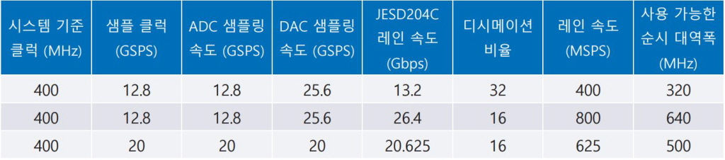
표 1은 400MHz 기준 클럭으로 구동되는 쿼드-아폴로 MxFE 시스템의 대표적인 세 가지 동작 설정을 요약한 것이다.
이들 설정은 샘플링 속도, 디지털 디시메이션, 데이터 처리량 간의 상호 트레이드오프를 보여주며, 서로 다른 시스템 요구사항에 맞춰 대역폭과 인터페이스 성능을 최적화하는 방법을 제시한다.
■ 차세대 레이더·전자전 아키텍처 구현·모사
쿼드-아폴로 MxFE X-밴드 디지털 빔포밍 플랫폼에 대한 시스템 레벨 검증을 통해, 모든 채널 전반에서 위상 코히어런트 동작이 확인되었으며, 1도 이하(sub-degree)의 위상 정렬 정확도와 피코초(ps) 이하의 타이밍 정확도를 달성했다.
적응형 빔 스티어링, 공간 널링(spatial nulling), 멀티빔 송신에서 보여준 성능은 이 플랫폼이 차세대 레이더 및 전자전 아키텍처를 구현 및 모사할 수 있는 준비가 되었음을 보여준다.
이러한 결과는 확장 가능한 모든 소자 기반 디지털 빔포밍 시스템을 실현하는 데 있어 중요한 이정표를 세운 것이다.
※ 저자 소개
싯다르타 다스(Siddhartha Das)는 미국 노스캐롤라이나주 더럼에 위치한 아나로그디바이스(Analog Devices) 항공우주·방산·통신(Aerospace, Defense, and Communications) 사업부 산하 서브시스템 및 센서팀의 시스템 애플리케이션 엔지니어다. 그는 2023년 버지니아 공과대학교에서 전기공학 학사 학위를 받았으며, 현재 동대학원에서 전기공학 석사 과정을 이수 중이다. ADI에서 싯다르타는 첨단 위상 배열 서브시스템의 개발, 통합, 특성 평가에 주력하고 있다. 그의 업무는 고성능 RF 신호 체인, 디지털 빔포밍 플랫폼, 멀티칩 동기화 기술 전반을 아우르며, 차세대 레이더 및 통신 시스템을 지원하는 데 중점을 두고 있다.

Comments
Related news
[Technical Contribution] ADI: "Multiphase Flyback Converter Delivers Over 60W of Power"
Frederik Dostal, a power management expert at Analog Devices, Inc., discusses the design of flyback converters for high-power applications.
2025.10.13by 명세환 기자
AI leaders commercialize four times faster than competitors and realize 50% higher value.
Global networking and cybersecurity technology company Cisco announced the "2025 Cisco AI Readiness Index," revealing that "Pacesetter" companies leading in AI adoption are achieving commercialization of pilots four times faster than competitors and realizing 50% higher value.
2025.10.15by 배종인 기자
ADI Unveils Power Studio, a Complete Power System Design Suite
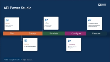
Analog Devices, Inc. (ADI) announced on the 24th through a press briefing that it will launch "ADI Power Studio," a comprehensive power design solution that provides advanced modeling, component recommendation, and efficiency analysis capabilities based on simulation. Additionally, ADI unveiled initial versions of "ADI Power Studio Planner" and "ADI Power Studio Designer," new web-based tools that deliver an enhanced user experience under the Power Studio brand.
2025.10.24by 배종인 기자
ADI Innovates AI Embedded Development and Upgrades Open-Source Development Platform
Global semiconductor company Analog Devices, Inc. (ADI) has officially announced 'CodeFusion Studio™ 2.0,' a major upgrade to its open-source embedded development platform. This update focuses on simplifying and accelerating AI-based embedded systems development while providing a developer-centric integrated toolchain.
2025.11.04by 명세환 기자
ADI, “Simple and Efficient Voltage Inverting Possible Without 'LTC7899' Transformer”
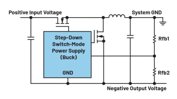
We spoke with Frederik Dostal, power management expert at Analog Devices, Inc., about voltage conversion ICs in inverting topology.
2025.11.06by 명세환 기자











