



ADI: "High-Precision Serial AVP Control μModule Regulator Transient Response Improvement"
 Published2026.02.05 16:09
LTM4650-2, 과도 응답 개선·출력 커패시터의 올-세라믹화·전력 소비 감소
통신 장비 및 데이터센터를 위한 전원 설계에서는 빠른 과도 응답과 소형화, 그리고 높은 전압 정확도를 동시에 만족시키는 것이 중요한 과제로 떠오르고 있다.
이러한 요구에 대응하기 위해 아나로그디바이스(ADI)의 μModule® 레귤레이터에 적용된 고정밀 직렬 방식 능동 전압 포지셔닝(AVP) 기법이 주목받고 있다.
이 방법을 활용하면 빠른 부하 과도 응답(transient response) 특성과 최소한의 보드 면적을 갖춘 올-세라믹(all-ceramic) 커패시터 기반의 전원 솔루션을 구현할 수 있다.
기존의 션트(shunt) 방식 AVP 구조와 비교했을 때, 이 직렬 AVP는 부하 라인(load line) 정확도가 매우 우수하며, 그 결과 출력 전압 정확도를 크게 향상시킨다.
사용자들에게 도움이 될 수 있도록 해당 기법을 적용한 실제 부하 과도 응답 측정 결과도 함께 제시한다.
■ 머리말
능동 전압 포지셔닝(AVP) 또는 능동 드룹(active droop) 제어는 부하 전류 크기에 따라 전원 출력 전압을 가변적으로 조정하는 기술이다.
경부하 조건에서는 출력 전압을 높게 유지하고, 중부하 또는 고부하 조건에서는 출력 전압을 낮추는 방식이다.
AVP 제어의 핵심 장점은 부하 과도 응답 성능을 개선하면서도 필요한 출력 커패시턴스를 줄일 수 있다는 점이다.
이는 전원 공급 장치가 급격한 부하 변화에 대응할 수 있는 전압 여유를 확보해 주기 때문이다.
μModule 레귤레이터는 사전 검증된 통합형 전원 모듈 솔루션으로, 통신 장비 및 데이터센터 애플리케이션에서 널리 사용된다.
이러한 시스템에서는 빠른 과도 응답, 최소한의 보드 면적, 그리고 올-세라믹 커패시터 솔루션이 선호된다.
하지만, 기존의 비-AVP(non-AVP) 제어 방식으로는 이 모든 조건을 충족하기가 어렵다.
이 글에서는 피드백 제어 루프에 두 개의 저항을 추가함으로써 고정밀 직렬 AVP를 구현하는 방법을 설명한다.
이 방식의 주요 이점은 부하 라인 특성이 gm 증폭기의 이득 편차에 거의 영향을 받지 않는다는 점이다.
반면, 션트 AVP1와 같은 다른 AVP 구현 방식은 gm 증폭기의 이득 변동이 클 경우, 부하 라인 정확도가 크게 저하될 수 있다.
직렬 AVP 기법을 적용하면, 출력 커패시턴스를 최대 50%까지 줄일 수 있으며, 출력 전압의 피크-투-피크 과도 응답 특성 역시 소폭 개선된다.
출력 커패시턴스 요구량이 감소함에 따라 세라믹 커패시터만으로 구성이 가능해진다.
세라믹 커패시터는 알루미늄 전해 커패시터에 비해 신뢰성이 훨씬 높고 가격도 저렴하기 때문에 시스템 신뢰성 향상과 비용 절감 측면에서도 유리하다.
또한 AVP 제어는 고부하 조건에서 출력 전압을 낮춤으로써 부하의 전력 소비를 줄이는 효과를 제공한다.
LTM4650-2 회로를 대상으로 한 실험 결과, 단일 출력 기준 1.4W, 전체 기준 5.6%의 전력 절감 효과가 확인되었으며, 이는 배터리 구동 시스템에서 사용 시간을 연장하는 데에도 기여한다.
■ 직렬 AVP 구현 원리
AVP는 부하 전류에 따라 출력 전압이 의도적으로 변화하도록 설계된 제어 방식이다.
기존 non-AVP 구조에서는 그림 1과 같이 모든 부하 조건에서 출력 전압이 명목 값(nominal VOUT)으로 유지된다.
하지만 AVP 방식을 적용하면 부하 전류가 증가할수록 출력 전압은 점점 더 낮아진다.
경부하 상태에서는 출력 전압이 명목 값보다 다소 높게 설정되며, 중부하 상태에서는 명목 값보다 약간 낮게 조정된다.
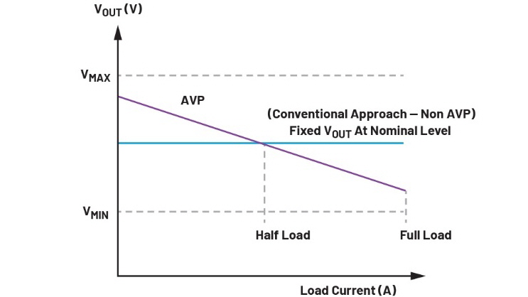
부하 전류가 갑자기 증가할 경우에는 출력 전압이 명목 값보다 높은 수준에서 시작되므로, 더 큰 드룹(droop)이 발생할 수 있고, 설정된 전압 범위 내에서 유지된다.
반대로 부하 전류가 급격히 감소하면 출력 전압은 명목 값보다 낮은 수준에서 시작하여 더 큰 오버슈트(overshoot)가 발생하지만, 이 역시 지정된 전압 범위(VMAX와 VMIN 사이) 내로 제한된다.
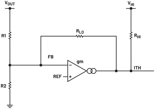
그림 2는 직렬 보상(series compensation) 방식의 AVP 회로를 보여준다.
▲그림 2. AVP 직렬 보상 회로
이 회로에서 내부 레퍼런스 전압(VREF)과 VOUT 피드백 신호는 오류 증폭기의 양(+) 및 음(-) 입력 단자에 각각 연결된다.
RHI에 인가되는 VHI (또는 INTVCC)는 출력이 포화 상태가 되지 않도록 증폭기 출력(ITH 또는 COMP)에 적절한 DC 전압을 공급한다.
피드백 저항(RLO)은 출력(ITH)에서 오류 증폭기의 음(-) 입력 단자(FB)로 연결되며, 이 RLO가 gm 증폭기의 이득에 가장 큰 영향을 미친다.
RHI와 RLO의 저항 값은 R1 및 R2보다 충분히 커야 한다.
부하 라인 공식 1은 다음과 같다:

여기서 Ki는 전류 감지 이득이며, RSENSE는 전류 감지 저항 값 또는 DCR 감지 방식에서의 인덕터 DCR 값을 의미한다.
AVP 션트 보상 회로1와 비교할 때, 직렬 보상 회로의 가장 큰 장점은 부하 라인이 R1/RLO 비율에 영향을 받으며, 오류 증폭기의 트랜스컨덕턴스(gm) 허용오차에는 거의 영향을 받지 않는다는 점이다.
반도체 공정의 특성상, 일부 IC의 gm 값은 제품에 따라 ±30%까지 차이가 날 수 있으며, 여기에 션트 보상 회로 AVP는 1/gm 이득에 정비례하기 때문에 이러한 변동에 취약하다.
■ LTM4650-2 적용 사례
LTM4650-2는 전류 모드 방식의 동기식 벅 μModule 레귤레이터로, 1V 출력에서 최대 25A의 부하를 공급할 수 있으며, 약 ±8% (160mVp-p)의 부하 과도 응답 창을 가진다.
기존 non-AVP 구성에서는 빠른 Type II 제어 루프 보상을 달성하기 위해 외부 RC 필터링 회로가 필요하다.
출력단에는 100μF 세라믹 커패시터 5개와 470μF POSCAP 2개가 사용됐다.
19A 부하 스텝(완전 부하의 75%)과 19A/μs의 슬루율 조건에서 측정된 출력 전압 과도 응답은 136mVp-p였다(그림 3).
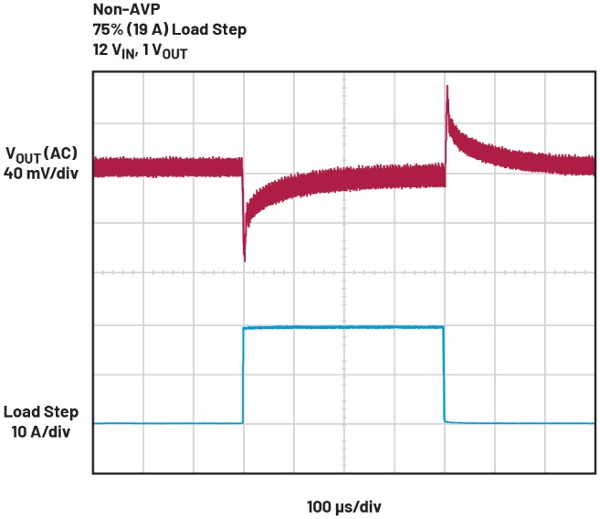
▲그림 3. Non-AVP 회로의 부하 과도 응답 파형. 136mVp-p의 출력 전압 과도 응답, COUT1 = 5× 100μF 세라믹, COUT2 = 2× 470μF POSCAP

▶ 과도 응답 성능 향상
AVP를 구현할 경우, AVP 보정 회로는 그림 4와 같이 COMP에 적용되지만, RC 보정은 필요치 않다. 절반의 부하(12.5A)에서, R2를 미세 조정함으로써 출력 전압을 명목 값(1V)으로 설정했다. 이때 부하 과도 응답은 95mVp-p로 측정되어(그림 5), 기존 방식보다 과도 응답 성능이 향상된 것을 확인할 수 있었다.
▶ 전력 절감 효과
출력 전압을 25A(완전 부하)에서 1V로 설정하면 부하 전력은 25W이지만, AVP를 적용해 0.945V로 낮출 경우, 부하 전력은 23.6W로 감소한다. 이로 인해 단일 출력 기준으로 1.4W, 듀얼 출력 기준 총 2.8W의 전력 절감 효과가 발생한다.
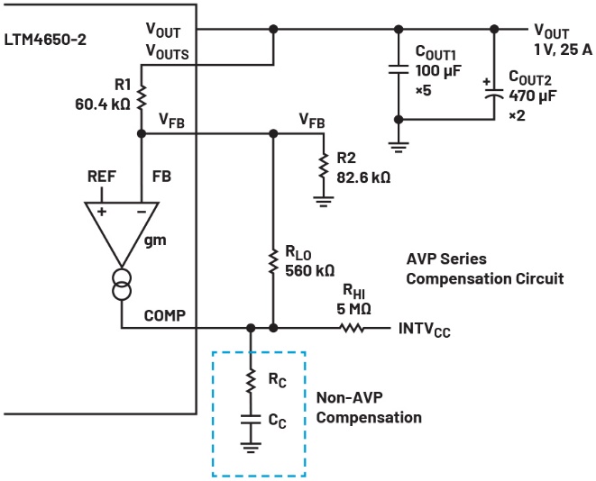
▲그림 4. AVP 적용 회로도(직렬 보상 회로)
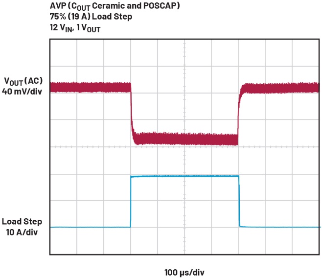
▲그림 5. 그림 4 회로에 AVP가 적용되었을 때의 부하 과도 응답 파형, 95mVp-p의 출력 전압 과도 응답. COUT1 = 5× 100μF 세라믹, COUT2 = 2× 470μF POSCAP.
▶ 올-세라믹 커패시터 구현
AVP를 구현하면, 기존 2개의 POSCAP을 2개의 세라믹 커패시터로 대체할 수 있으므로 총 7개의 100μF 세라믹 커패시터가 COUT1에 사용된다. 세라믹 커패시터를 사용할 경우, 낮은 등가 직렬 저항(equivalent series resistance, ESR), 낮은 등가 직렬 인덕턴스(equivalent series inductance, ESL), 비용 절감, 더 작은 크기, 더 높은 신뢰성 등의 장점을 얻을 수 있다. 과도 응답 성능이 향상되었고, 측정 결과는 그림 6에서와 같이 VOUT 과도 응답이 104mVp-p였다.
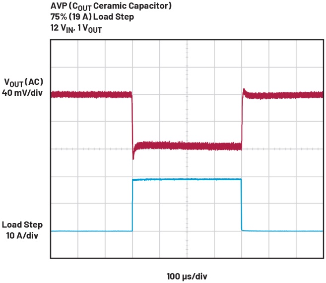
▲그림 6. AVP가 적용된 회로의 부하 과도 응답 파형, 104mVp-p의 출력 전압 과도 응답. COUT1 = 7× 100μF 세라믹 커패시터
표 1은 Non-AVP(기준치), AVP, 그리고 비교를 위해 출력 세라믹 커패시터만을 사용한 AVP의 부하 과도 응답 Vp-p 측정값을 비교한 것이다.
.jpg) 표 1. Non-AVP, AVP, 그리고 출력 세라믹 커패시터만 사용한 AVP 간의 부하 과도 응답(Vp-p) 비교
표 1. Non-AVP, AVP, 그리고 출력 세라믹 커패시터만 사용한 AVP 간의 부하 과도 응답(Vp-p) 비교■ 결론
LTM4650-2 μModule 레귤레이터에 AVP 직렬 보상 회로를 구현한 결과, 부하 과도 응답 특성이 개선되었으며, 고부하 조건에서 부하 전력 소비가 감소했다.
출력 커패시턴스는 절반 이하로 줄어들었고, POSCAP을 세라믹 커패시터로 대체함으로써 비용 절감과 보드 면적 최소화가 가능해졌다.
이 AVP 기법은 외부 RC 보상 네트워크를 갖춘 외부 보상 핀을 가진 다른 μModule 레귤레이터(예: LTM4630-1, LTM4626, LTM4636, LTM8055-1 등)에도 적용할 수 있다
※ 저자 소개
신 켕 리(Sin Keng Lee)는 2022년 5월에 아나로그디바이스(ADI)에 입사하여 ADI의 전력 모듈 설계 엔지니어로 재직중이다. 그는 영국 노섬브리아 대학교에서 안테나, RF 및 마이크로파 통신 공학 학사 및 박사 학위를 취득했다.
지준 치안(Zhijun (George) Qian)은 아나로그디바이스의 전원 모듈 설계 담당 선임 매니저로, LTM80xx 전 제품과 LTM46x/LTM47x 일부 제품을 담당하고 있다. 저장대학교에서 학사 및 석사학위를, 센트럴 플로리다대학교에서 전력전자 박사 학위를 취득했다. 2010년 초에 ADI에 입사했다.

Comments
Related news
[Technical Contribution] ADI: "Multiphase Flyback Converter Delivers Over 60W of Power"
Frederik Dostal, a power management expert at Analog Devices, Inc., discusses the design of flyback converters for high-power applications.
2025.10.13by 명세환 기자

AI leaders commercialize four times faster than competitors and realize 50% higher value.
Global networking and cybersecurity technology company Cisco announced the "2025 Cisco AI Readiness Index," revealing that "Pacesetter" companies leading in AI adoption are achieving commercialization of pilots four times faster than competitors and realizing 50% higher value.
2025.10.15by 배종인 기자
ADI Unveils Power Studio, a Complete Power System Design Suite
Analog Devices, Inc. (ADI) announced on the 24th through a press briefing that it will launch "ADI Power Studio," a comprehensive power design solution that provides advanced modeling, component recommendation, and efficiency analysis capabilities based on simulation. Additionally, ADI unveiled initial versions of "ADI Power Studio Planner" and "ADI Power Studio Designer," new web-based tools that deliver an enhanced user experience under the Power Studio brand.
2025.10.24by 배종인 기자

ADI Innovates AI Embedded Development and Upgrades Open-Source Development Platform
Global semiconductor company Analog Devices, Inc. (ADI) has officially announced 'CodeFusion Studio™ 2.0,' a major upgrade to its open-source embedded development platform. This update focuses on simplifying and accelerating AI-based embedded systems development while providing a developer-centric integrated toolchain.
2025.11.04by 명세환 기자
ADI, “Simple and Efficient Voltage Inverting Possible Without 'LTC7899' Transformer”
We spoke with Frederik Dostal, power management expert at Analog Devices, Inc., about voltage conversion ICs in inverting topology.
2025.11.06by 명세환 기자











