



Applied Materials Acquires NEXX… Expanding Panel-Based Advanced Packaging Capabilities
 Published2026.05.07 09:33
.jpg)
Strengthening panel-level processes and supplementing deposition technology portfolio amid the trend toward larger AI chips
Applied Materials has decided to acquire the NEXX business unit, a semiconductor packaging equipment company. Through this, the company plans to secure advanced large-area packaging process technology and expand its related equipment portfolio.
This agreement was announced on May 7 and is expected to be finalized within a few months following standard procedures. The transaction is structured to proceed without separate regulatory approval.
NEXX is a company that has supplied deposition equipment applied to large-area substrates in the semiconductor packaging process. In particular, it possesses electrochemical deposition (ECD) technology suitable for panel-unit processes, and is classified as a technology group that can complement existing wafer-based manufacturing.
With the recent expansion of demand for AI computing, designs integrating GPUs, high-bandwidth memory (HBM), and I/O chips into a single package are increasing. Consequently, 2.5D and 3D chiplet technologies are becoming widespread, and wider interposers and substrates are required. In the industry, there is a growing trend of gradually expanding the transition from existing 300mm wafer-centered production to panel-unit processes of 500mm or larger.
Applied Materials has been supplying equipment covering various processes, including lithography, PVD, CVD, etching, and inspection. With the addition of panel-level deposition technology, the company has expanded its scope to encompass the entire large-scale package manufacturing process. The company explained that it plans to pursue process optimization, such as fine wiring formation, through this acquisition.
A company official stated that the acquisition of NEXX is expected to bring technological complementarity in the field of panel-based advanced packaging and is also anticipated to influence the expansion of joint development with clients. NEXX also announced that it plans to focus on maintaining product competitiveness and improving quality following the integration, based on its existing technologies.
The industry views this deal as having taken place in conjunction with the competition in AI semiconductor packaging technology. As chip design complexity increases, manufacturing processes are shifting toward larger areas and higher densities, and competition among equipment manufacturers to secure the necessary technology to respond to this trend is expected to continue.
Following the completion of the transaction, the NEXX organization will be incorporated into Applied Materials’ semiconductor product group and will continue to operate based in Billerica, Massachusetts, as before.

Comments
Related news
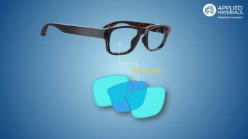
Applied Materials and GlobalFoundries Partner to Develop AI-Based Photonics
Applied Materials has entered into a strategic partnership with GlobalFoundries and will establish a state-of-the-art waveguide manufacturing facility in Singapore. This collaboration is aimed at accelerating technological innovation in AI-based photonics, and the two companies plan to jointly develop high-performance optical solutions for implementing next-generation digital experiences by combining their expertise in semiconductors and materials engineering.
2025.10.02by 명세환 기자
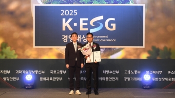
Applied Materials Recognizes Sustainability Through ESG
Applied Materials Korea (CEO Park Kwang-seon) received both the 'Grand Prize in ESG Division' and the 'Minister of Foreign Affairs Award' at the '2025 K-ESG Management Awards' ceremony, establishing itself as a model company for sustainable management.
2025.10.22by 명세환 기자

Applied Materials Establishes Applied Collaboration Center Korea in Osan
Applied Materials, a global leader in semiconductor and display materials engineering solutions, is establishing the 'Applied Collaboration Center Korea' in Gasan-dong, Osan, Gyeonggi Province, and accelerating the development and commercialization of next-generation semiconductor technologies that will lead the artificial intelligence (AI) era.
2025.11.21by 배종인 기자
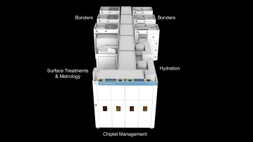
Applied Materials Accelerates AI Semiconductor Manufacturing Innovation
Applied Materials, a global leader in semiconductor and display materials engineering solutions, introduced Kinex bonding systems, Centura Xtera epi systems, and PROVision 10 electron beam metrology systems, targeting key areas of AI chip development competition including △advanced logic based on GAA (gate-all-around) transistors △HBM (high-bandwidth memory) DRAM △advanced packaging for implementing highly integrated system-in-package (SiP).
2025.11.27by 배종인 기자
.jpg)
Applied Materials to Unveil Energy-Efficient AI Semiconductor Technology at SEMICON Korea 2026
Applied Materials Korea, a leader in advanced semiconductor and display materials engineering solutions worldwide, will participate in 'Semicon Korea 2026' held at Seoul COEX from February 11 to 13, and will unveil key technologies for energy-efficient AI computing.
2026.01.29by 배종인 기자











