


SK Hynix Unveils Next-Generation AI Infrastructure Blueprint Based on Optical Interconnect
 Published2026.08.21 11:06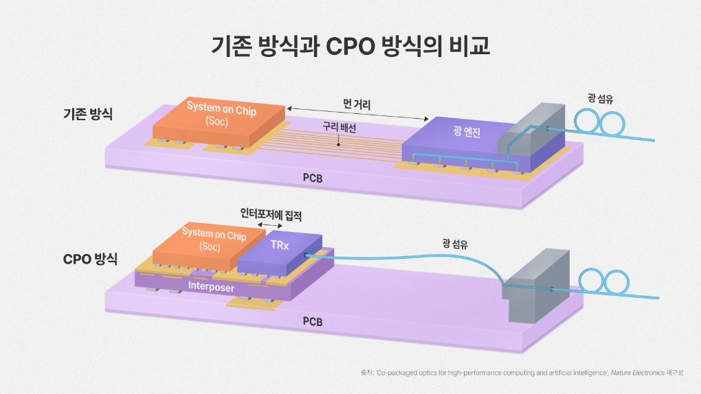
HBM 넘어 랙·포드 단위 데이터 병목 해결 제시
AI 반도체 경쟁의 무게중심이 개별 칩 성능에서 시스템 전체 최적화로 이동하는 가운데, SK하이닉스가 차세대 AI 인프라 핵심 기술인 CPO(Co-Packaged Optics) 로드맵을 제시했다.
SK하이닉스는 글로벌 연구진과 공동으로 AI 및 고성능 컴퓨팅(HPC)을 위한 광 인터커넥트 기술인 CPO의 발전 방향을 담은 논문을 국제 학술지 네이처 일렉트로닉스(Nature Electronics)에 게재했다고 최근 밝혔다.
이번 연구에는 SK하이닉스 AI 인프라 부문의 홍승훈 팀장과 미국 버지니아대학교 이규상 교수가 교신저자로 참여했으며, 일리노이대학교 어바나-샴페인(UIUC), MIT, 난양공과대학교(NTU), 연세대학교 연구진이 공동 참여했다.
논문은 생성형 AI 확산으로 수천 개의 GPU와 HBM이 연결된 초대형 AI 클러스터가 등장하면서 시스템 간 데이터 이동이 새로운 성능 제한 요소로 부상했다고 분석했다.

연산 성능은 빠르게 향상되는 반면 시스템 간 데이터 전송 대역폭 증가는 상대적으로 제한되면서 이른바 ‘대역폭 장벽(Bandwidth Wall)’ 현상이 심화되고 있다는 설명이다.
기존 구리 기반 전기 인터커넥트는 거리 증가에 따라 신호 손실과 전력 소모가 커지는 문제가 있다. 연구진은 이를 해결하기 위한 방안으로 광 송수신기를 프로세서와 동일 패키지에 집적하는 CPO 기술을 제시했다.
논문은 장기적으로 광 연결 기술을 메모리 인터페이스까지 확대하는 ‘옵틱스 중심(Optics-Centric) 아키텍처’ 개념도 제안했다.
광 인터포저를 통해 프로세서와 메모리를 직접 연결하면 여러 AI 가속기가 대규모 메모리 자원을 공유할 수 있어 AI 모델 규모 확대와 데이터 이동 효율 개선에 도움이 될 수 있다는 것이다.
연구진은 차세대 AI 인프라 구현을 위해 노드당 100Tb/s 이상의 대역폭, 1pJ/bit 미만의 에너지 소비, 10ns 미만의 칩 간 지연시간 등을 주요 기술 목표로 제시했다.
SK하이닉스는 이번 연구가 HBM과 같은 개별 메모리 기술을 넘어 메모리, 패키징, 광 인터커넥트 기술을 통합한 시스템 수준의 AI 인프라 발전 방향을 제시한 데 의미가 있다고 설명했다.

Comments
Related news
.jpg)
The Future of AI Data Centers, Why CPO Now?… e4ds EEWebinar to be held on July 21
e4ds news will host a webinar on July 21st through the e4ds EEWebinar titled 'Why CPO Now? The Future of Data Center Optical Interconnects'. Advisor Im Seung-chan, who will present at this webinar, plans to introduce the technical limitations faced by data centers in the AI era and the development direction of next-generation optical interconnect technology.
2026.07.08by 배종인 기자
.jpg)
The Era of 1 Million GPUs: Bottlenecks Are 'Wiring,' Not Computation… CPOs Are Changing the Data Center Landscape
AI data centers face data movement as a bottleneck rather than GPU computation. CPO (Co-Packaged Optics), which packages switch ASICs and optical engines together, is emerging as a key technology to reduce copper wiring limitations and address power and latency issues.
2026.07.31by 배종인 기자
The Future Opened by the Convergence of Light and Semiconductors…'Optical Science and Optical Semiconductor Workshop 2026' Held in Suwon
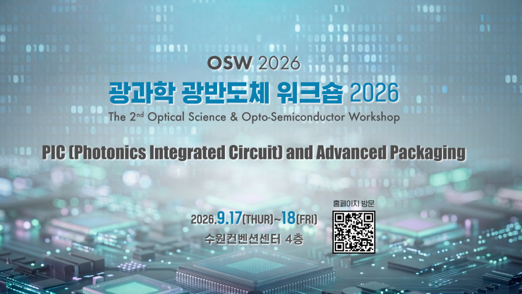
The 'Optical Science and Optical Semiconductor Workshop 2026' addressing light and semiconductor convergence technologies will be held on September 17-18 at the Suwon Convention Center. This year's theme is Photonic Integrated Circuits (PIC) and advanced packaging, with keynote presentations by Dr. Shin Dong-jae from imec and Professor Choi Woo-young from Yonsei University. Next-generation optical semiconductor technologies including PIC-EIC co-design and ultra-dense WDM receivers will be discussed, with presentations in 8 fields covering PIC platforms, processes, high-speed devices, signal and power integrity, as well as packaging processes, equipment, materials, and verification. Paper submissions are accepted from July 28 to August 24, and advance registration runs until September 7.
2026.08.21by 배종인 기자

Arm Announces CPU Benchmarking Methodology for Agentic AI
Arm has announced a CPU performance evaluation methodology specialized for agentic AI workloads. Developed with support from Fujitsu, Meta, and OpenAI, this methodology focuses on performance measurement based on actual agent task completion results. According to independent verification by Signal65, the Arm AGI CPU demonstrated an average performance advantage of 1.99x per rack compared to AMD EPYC Turin, with performance differences of 1.7x to 2.2x particularly in the tooling, orchestration, and inference domains.
2026.10.15by 배종인 기자
Panasia Accelerates CXL Appliance Deployment at OCP Global Summit 2026
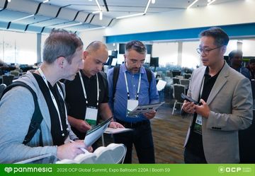
Panasia unveiled a complete CXL server rack solution based on PCIe 6.4-CXL 3.2 fusion switch technology at OCP Global Summit 2026. As memory demand increases with the proliferation of agentic AI, Panasia's solution integrates CPU, memory, and accelerators into a single fabric, enabling large-scale CXL environments to be configured without separate testing. Hyperscalers have reported results of reducing server counts by up to 25% through CXL memory deployment, and Panasia expects to accelerate the timeline for datacenter CXL adoption through collaboration with major system manufacturers.
2026.10.15by 배종인 기자











