



TSMC·ASML Promote Transition to 12-inch Photomasks for High NA EUV...Target Mass Production in 2033
 Published2026.09.09 04:14
2031년 파일럿 라인 구축 추진
TSMC와 ASML이 차세대 반도체 제조 기술인 High NA EUV(극자외선) 노광공정의 생산성 향상을 위해 대형 포토마스크 전환 협력을 추진한다. 양사는 현재 사용 중인 6인치 포토마스크를 12인치 규격으로 확대해 차세대 공정의 생산성과 비용 경쟁력을 높인다는 계획이다.
TSMC와 ASML은 8일 High NA EUV용 12인치 포토마스크 전환을 위한 공동 산업 이니셔티브를 출범했다고 밝혔다. 양사는 2031년 12인치 포토마스크 파일럿 라인을 구축하고, 2033년에는 관련 노광 시스템을 첨단 공정 양산에 적용하는 것을 목표로 하고 있다.
EUV 노광은 첨단 반도체 제조에 활용되는 핵심 공정 기술이다. High NA EUV는 기존 EUV보다 더 높은 해상도를 구현해 미세 공정 구현에 활용된다.
양사에 따르면 향후 High NA EUV는 현재 사용되는 6인치 포토마스크로 먼저 양산에 적용된 이후 12인치 포토마스크로 확대될 예정이다.
12인치 포토마스크가 도입되면 생산성 향상과 제조 비용 절감, 스티칭(Stitching) 제약 해소 등이 가능해질 것으로 기대된다. 또한 첨단 반도체 제조업체들이 High NA EUV의 성능을 보다 효율적으로 활용할 수 있도록 지원할 전망이다.

크리스토프 푸케 ASML 최고경영자(CEO)는 “12인치 포토마스크는 더 높은 스캐너 생산성을 제공하고, 더 작고 빠르며 에너지 효율적인 반도체 수요에 대응하는 데 도움이 될 것”이라고 말했다.
TSMC는 2030년부터 첨단 공정 양산에 ASML의 High NA EUV 기술을 도입할 계획이라고 밝혔다.
회사에 따르면 AI 관련 반도체 설계가 복잡해지면서 High NA EUV가 필요한 공정층 수가 증가할 것으로 예상된다. 이에 따라 향후 대형 포토마스크 전환의 필요성도 확대될 것으로 보고 있다.
양사는 미국 캘리포니아주 몬터레이에서 열린 SPIE BACUS 콘퍼런스에 앞서 관련 협력 체계를 구축했다. 주요 반도체 제조사와 포토마스크 공급업체, 장비·소재 기업들도 이번 프로젝트 참여 의사를 나타냈다고 설명했다.
TSMC의 웨이저자(C.C. Wei) 회장 겸 CEO는 “산업 전반의 협력을 통해 첨단 기술의 혜택을 보다 넓게 제공할 수 있을 것으로 기대한다”고 밝혔다.

Comments
Related news

Samsung Electronics Expands High NA EUV and 12-inch Mask Collaboration with ASML
Samsung Electronics is expanding its collaboration with ASML to secure next-generation lithography technology. The company is pursuing joint development of 12-inch photomasks and introduction of High NA EUV into D-RAM mass production processes by 2028. Through the transition to 12-inch masks, the company expects to eliminate stitching constraints and improve productivity, while expanding High NA EUV application to the memory sector to simultaneously achieve D-RAM miniaturization and process simplification.
2026.09.08by 배종인 기자
Intel Foundry and ASML Achieve Breakthrough in High NA EUV Application to Over 1 Million Wafer Processes
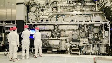
Intel Foundry and ASML have disclosed their mass production achievements with High NA EUV lithography technology. To date, High NA EUV has been applied to over 1 million wafer processes, and is currently being utilized in mass production of certain layers of Panther Lake processors. The two companies are strengthening industry cooperation for near-term support based on 6-inch masks and future transition to 6×12-inch masks.
2026.09.08by 배종인 기자
ASM Participates in Semiconductor Scholarship Program for Fifth Consecutive Year…Supporting Science and Engineering Talent
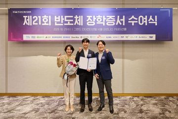
ASM, a semiconductor deposition equipment specialist, participated in the "21st Semiconductor Scholarship Certificate Presentation Ceremony" organized by the Korea Semiconductor Industry Association and presented scholarship certificates to graduate students at Ulsan National Institute of Science and Technology. ASM has been supporting the KSIA scholarship program for five consecutive years since 2022 and is currently conducting multilayered talent development activities including donations to the Hwaseong City Foundation, global exploration programs, and mentoring for women in science and engineering.
2026.10.23by 배종인 기자
KERI Redefines SiC Semiconductor Defect Luminescence Wavelength After 15 Years
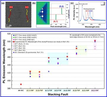
The Korea Electrotechnology Research Institute has corrected the international standard for distinguishing stacking defects in SiC power semiconductors for the first time in 15 years. Through atomic-level analysis, they have demonstrated that the luminescence wavelength previously known as 424nm is actually 459nm, establishing grounds for revising the IEC standard. This is expected to contribute to improving the accuracy of quality inspection for power semiconductors used in electric vehicles and renewable energy equipment.
2026.10.23by 배종인 기자
Korea Institute of Materials Science Develops Core Technology for High-Performance Permanent Magnets Without Heavy Rare Earths
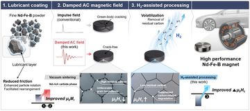
The Korea Institute of Materials Science has developed core technology to manufacture high-performance permanent magnets without using heavy rare earths. This technology, which secures integrated process technology from the production of approximately 1μm-sized Nd-Fe-B ultrafine powder to alignment and sintering, is applicable to electric vehicle drive motors and industrial robots, and is expected to reduce supply chain dependence on rare earth magnets and accelerate domestic material localization.
2026.10.23by 배종인 기자











