



Applied Materials and Besi Expand AI Packaging Partnership
 Published2026.10.02 09:14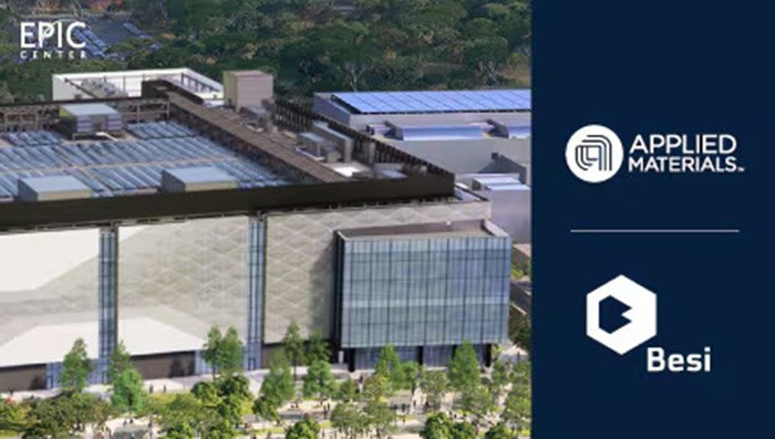
The expanded cooperation is characterized by broadening the scope of joint development beyond the existing die-to-wafer hybrid bonding collaboration to include new hybrid bonding platforms, thermocompression bonding (TCB) scaling, die-on-wafer, die-on-die, die-on-panel integration, and photonics-based interconnects.
The EPIC Center is the largest advanced semiconductor R&D facility in the United States, established with approximately $5 billion in investment, and is scheduled to be operational by year-end.
Capital expenditures will be expanded progressively as customer projects commence.
Richard Blickman, CEO of Besi, stated, "We will advance TCB scaling, die-on-panel integration, and interconnect technologies for next-generation AI and photonics systems."

Comments
Related news
.jpg)
Applied Recognized for Community Contribution
Applied Materials Korea received the Grand Prize in the Community Contribution category at the '2026 Korea Chamber of Commerce and Industry and Forbes Corporate Social Responsibility Awards'. The company was recognized for its continued efforts in citizen-participated river cleanup activities, science education for children, traditional culture experiences, and support for semiconductor talent development.
2026.05.28by 명세환 기자
Applied Materials Unveils Deposition and Selective Etching Systems for 3D Semiconductor Processes
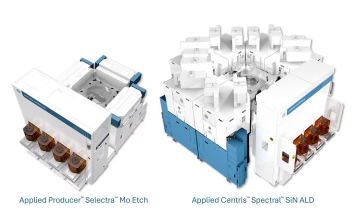
Applied Materials has unveiled new deposition and selective etch equipment to address 3D semiconductor structures with increased complexity due to AI semiconductor proliferation. The newly announced Centris Spectral SiN ALD system supports uniform silicon nitride film formation in high-aspect-ratio structures, while the Producer Selectra molybdenum etch system provides selective metal removal processes for wordline separation in 3D NAND. Both tools are focused on enhancing material control precision in logic and memory processes to support performance and yield improvement of next-generation semiconductors.
2026.06.16by 배종인 기자
Applied Technologies Unveils 6 Semiconductor Equipment Models Supporting 3D Chip Architecture
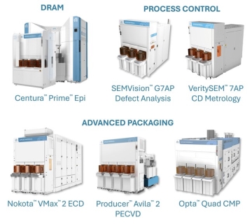
Applied Materials has unveiled six new semiconductor manufacturing equipment solutions to address growing AI computing demands and the expansion of 3D stacking structures and HBM technology. The lineup consists of three advanced packaging process tools—Opta Quad CMP, Nokota Vmax 2 ECD, and Producer Avila 2 PECVD—along with two electron beam metrology systems, VeritySEM 7AP and SEMVision G7AP, and one Centura Prime epi system.
2026.06.29by 배종인 기자
Applied, Green Umbrella Foundation Supports AI and Semiconductor Education
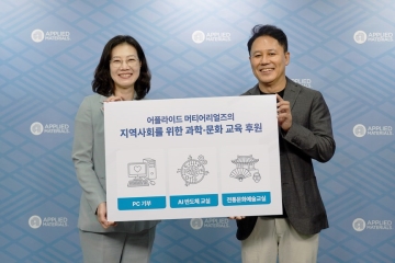
Applied Materials Korea has partnered with the Green Umbrella Children's Foundation to provide AI and semiconductor experiential education as well as traditional cultural and arts education to children in four regions of Gyeonggi Province. The company will offer convergence education utilizing AI vision sensors and semiconductor STEM kits, with approximately 330 elementary school students and children from community child centers expected to participate. Additionally, Applied Materials Korea will donate 90 laptops and 12 speakers to 67 community child centers to improve the digital learning environment.
2026.07.23by 배종인 기자
Applied Materials Records Q3 Revenue of $9.1 Billion…Quarterly Record
Applied Materials achieved record quarterly revenue of $9.1 billion in fiscal 2026 Q3. Driven by expanding AI demand, the company grew 25% year-over-year, achieving record operating margin of 33.7% and Non-GAAP EPS of $3.50. The semiconductor systems segment increased 26.5% to $7.0 billion, led by foundry and logic at 67%.
2026.08.14by 배종인 기자











