


ams Updates Schedule for IC Prototype Service '2016 Official Service'
 Published2015.11.13 15:27
MPW, a prototype service, integrates multiple designs from different customers onto a single wafer, and because wafer and mask costs are shared with other shuttle participants, foundry customers can enjoy significant cost benefits.
Shuttle participants can also utilize the recently announced high-voltage transistor service with excellent voltage scalability. Optimized for a wide range of drain-source voltage (VDS) levels from 20V to 100V and offering significantly low on-resistance, this highly scalable transistor results in a substantial reduction in area compared to standard transistors. Foundry customers developing complex high-voltage analog/mixed-signal applications can immediately benefit from a greater number of dies per unit area.
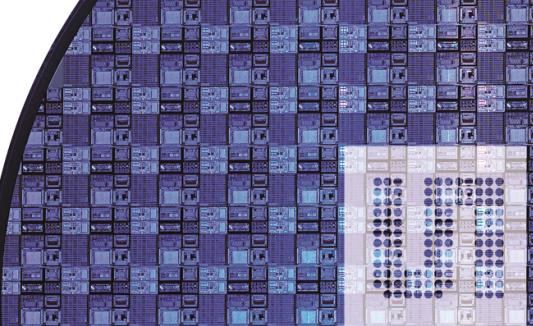 ams’s MPW services, which are the best in the industry, provide the full range of specialized process technologies for 0.18μm and 0.35μm. To provide leading analog semiconductor process technology, manufacturing, and services, ams offers four MPW runs (RUN: a unit specified in the FAB process, typically 24 to 25 wafers per RUN) of the 0.18μm CMOS (C18) process, as well as four MPW runs of state-of-the-art 0.18μm high-voltage CMOS (H18) technology supporting 1.8V, 5V, 20V, and 50V devices.
For the 0.35μm professional process, a total of 14 runs will be available in 2016. ams’s 0.35μm high-voltage CMOS process family is optimized for high-voltage designs in automotive and industrial applications and supports 20V, 50V, and 120V devices, as well as transistors with true voltage scalability. In addition to advanced high-voltage CMOS processes with embedded EEPROM capabilities, the 0.35μm SiGe-BiCMOS technology S35 is fully compatible with basic CMOS processes and complements ams’s MPW service portfolio.
Overall, ams can interoperate with leading global partner organizations such as CMP, Europractice, Fraunhofer IIS, and Mosis, and plans to provide approximately 150 MPW service launch schedules in 2016. Customers located in the Asia-Pacific region can also participate through the region's MPW program partners, Toppan Technical Design Center Co., Ltd (TDC) and MEDs Technologies.
Please check the website for detailed start dates for each process.
The schedule for 2016 has now been released, and detailed start dates for each process can be found on the website www.ams.com/MPW.
To take advantage of the MPW service, ams’s foundry customers provide GDSII-data completed on a specific date and receive untested package samples or dies within a short lead time of typically 8 weeks for CMOS or 12 weeks for high-voltage CMOS, SiGe-BiCMOS, and embedded flash processes.
All process technologies are supported by the well-known heat kit, ams’s industry benchmark process design kit. This design kit is based on the Cadence, Mentor Graphics, or Keysight ADS design environments. This heat kit is supplied with standard cells and peripheral cells that are fully verified as semiconductors, as well as general-purpose analog cells such as comparators, operational amplifiers, and low-power A/D and D/A converters.
Custom analog and RF devices, physical verification rule sets suitable for Assura and Calibre, as well as precisely characterized circuit simulation models, enable the rapid design start of complex high-performance hybrid ICs. In addition to standard prototyping services, ams also provides state-of-the-art analog IP blocks, memory (RAM/ROM) generation services, and ceramic or plastic packaging services.
Comments
Related news

ams Expands Process Portfolio to Include CMOS Optoelectronics Foundry, Delivering Value Beyond Semiconductors
This platform represents a portfolio expansion for ams' pursuit of "More Than Silicon" value realization, and follows the approach of providing technology modules, IP (Intellectual property), cell libraries, engineering consultants, and service packages based on ams' specialized technologies to enable customers to successfully develop state-of-the-art analog and mixed-signal circuit designs.
2015.08.13by 명세환 기자
ams Korea, Expanded Relocation and Domestic Business Strengthening Meeting
ams Korea, the Korean subsidiary of ams, a specialist in high-performance analog ICs and sensors, announced that it has expanded and relocated its office to Pangyeon-ro in Seongnam-si, Gyeonggi Province. With its new establishment in Pangyo Techno Valley, ams Korea required expanded workspace due to personnel recruitment following growth in the sensor market and expansion of domestic business activities, as well as enhanced customer support infrastructure. Through this office expansion and relocation, ams Korea has established a foundation to strengthen collaborative relationships by providing specialized technical support services to customers more rapidly, and to solidify its position as a sensor specialist in the domestic market.
2015.07.21by 신윤오 기자

What is ams' IC used in a small wearable scanner?
ams announced that Technology Solutions Limited (TSL), a British company, has integrated ams's highly integrated, low-power reader IC (product name: AS3993) into its new wearable-type RFID scanner product 1153. Technology Solutions stated, "The requirements for efficient read performance with very low power consumption were a clear justification for our adoption of ams's AS3993."
2015.10.07by 명세환 기자

Intel Unveils Next-Generation 'Core Ultra Series 3' and vPro Platform for Enterprise PCs
Intel has officially unveiled the "Intel Core Ultra Series 3" for next-generation enterprise PCs and the latest vPro platform, addressing a wide range of demands from enterprise notebooks to high-performance workstations.
2026.03.26by 배종인 기자

ROHM Launches ESD Protection Diode Compatible with High-Speed Interfaces of 10Gbps or Higher
Semiconductor specialist ROHM has developed the 'RESDxVx series' of ESD (electrostatic discharge) protection diodes capable of responding to next-generation high-speed data communication environments exceeding 10Gbps, simultaneously enhancing both signal quality maintenance required in high-speed interfaces and IC protection performance.
2026.03.26by 배종인 기자











