


How far has the development of core sensor elements come? ① “We will compete with overseas companies by developing the smallest 9-axis sensor”
 Published2015.11.16 21:52
The government plans to support a total of KRW 150.8 billion (KRW 114.8 billion from the national budget) from this year to 2020 to intensively foster image sensors, magnetic sensors, inertial sensors, pressure sensors, radar sensors, environmental sensors, optical sensors, infrared sensors, acoustic sensors, and bio-medical sensors.
By examining the development status and development goals of these sensors, we assessed the competitiveness of the domestic sensor industry. This week, we will introduce the technologies selected for the sensor industry advanced technology development, including ▲9-axis smart motion sensor ▲metabolic volume measurement system ▲ultra-small hazardous gas sensor ▲optical sensor, and next week, in Part 2, we will introduce ▲vehicle shunt resistance current sensor ▲autonomous vehicle lidar sensor ▲79GHz vehicle radar sensor technology.
6-axis 9-axis smart motion sensor, size and price reduced
Compete with the top three overseas companies (InvenSense, ST, Bosch) by developing cutting-edge smart motion sensors.
The development of the 9-axis smart motion sensor core technology was led by Shinsung C&T, with the participation of about 10 schools and institutions, including Seoul National University and Crayon Technologies.
This project aims to reduce the size and unit price by 10% to 30% compared to overseas competitors by manufacturing a pilot-scale prototype of the world's smallest 9-axis smart motion sensor, a pilot-scale prototype of the world's smallest single-chip 6-axis inertial sensor based on semiconductor TSV, and a pilot prototype of the world's smallest 3-axis geomagnetic sensor.
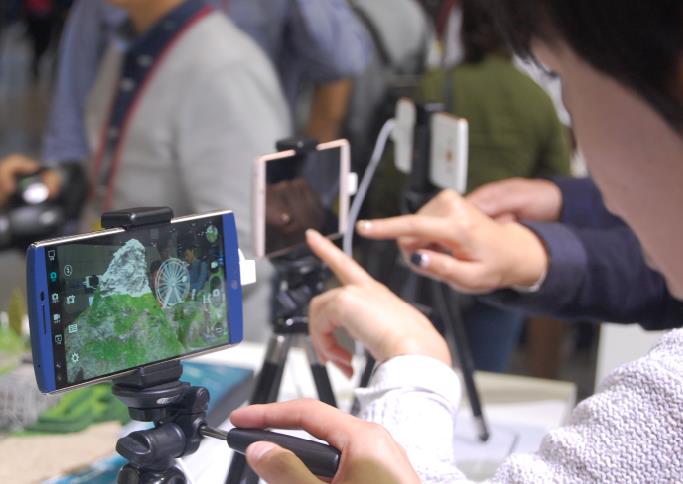
▲Smartphones have become a collection of various cutting-edge sensors. The photo shows visitors looking at the latest smartphones at an exhibition.
The key to differentiating from overseas competitors is semiconductor TSV technology. Like the three major overseas companies, it applies multi-space sealed wafer-to-wafer package acceleration/gyro applications, gyro sensing part x, y gyro z gyro applications, MEMS-SoC wafer-to-wafer stacking packages, etc., but the strategy is to differentiate with a semiconductor TSV-based MEMS gyroscope.
In addition, the 6-axis inertial sensor technology is also planned to reduce package size by 30%, current consumption by 10%, and manufacturing cost by 30% compared to overseas competitors. 3-axis gyroscopes, 6-axis inertial sensors, and 9-axis smart motion sensors are essential components for smartphones and automobiles, and the technological difficulty is high, making it difficult for domestic companies to enter the market. It is analyzed that if these sensors are successfully commercialized, it can bring about import substitution and a large increase in exports.
In the future, we will supply 9-axis sensors to major domestic companies by replacing imported ones.
“In order to achieve this goal, we need to solve the following problems: sensitivity degradation due to miniaturization of the 6-axis inertial sensor; sensitivity deviation due to MEMS process errors and external environmental changes due to miniaturization; WB pad size space and multi-chip package manufacturing cost; and sensor capacitance value reduction,” said Yongguk Kim, head of research at Shinsung C&T.
In addition, CEO Kim stated, “Since there is currently no company developing a 9-axis sensor in Korea, we have selected the sensor sector as a key area for future corporate growth and will invest 2 billion won in the 9-axis sensor development sector.” The company plans to supply 9-axis sensors to major domestic companies in the future by replacing imports.
Dongkuk Innotech Co., Ltd. is the main organization developing a metabolic measurement system capable of simultaneous analysis of multiple variables (pH, dissolved oxygen, calories) of 1,000 or fewer cell samples. This project aims to develop a multivariate sensor system for measuring cell metabolism and commercialize it within three years. The product technology is to develop a high-sensitivity pH, O2, and heat sensor using BioMEMS and Microfluidic technologies and to systemically integrate and commercialize it.
Preempting BioMEMS technology with a narrow technology gap with advanced countries
Dongkuk Innotech's Research Institute Director Lee Jong-mok said, "Unlike products from advanced overseas companies, the fact that it measures calories is its competitive edge," and "Since it simultaneously measures three major variables related to cell metabolism in real time, which did not previously exist, the prospects for patent registration are bright." Through this technology, the burden of sensor maintenance and consumable purchase costs is reduced by miniaturizing and integrating the sensor, and experiments are possible with a smaller number of cells compared to existing technologies that require at least 10,000 cells. Another advantage is that the application of microfluidic technology can resolve restrictions and inconveniences in cell maintenance, such as the inability to exchange and supply CO2 under closed experimental conditions.
The head of this division said, “There is an effect in developing a new biosensor system with BioMEMS technology, which has a small technological gap with advanced countries,” and “In particular, we emphasize the differentiation of multivariate measurement and functionality specialized for drug screening, and we emphasize differentiation of automation functions compared to competitors, which enable us to provide stable supply of consumables at a lower price and immediate technical support.”
The development of the U-sensor, an ultra-small hazardous gas sensor system based on floating multi-nano elements, was led by Professor Lee Yoon-sik of Ulsan National University of Science and Technology. U-Sensor is a collective term for sensor technology and products that have secured global competitiveness, including components, materials, chips, modules, and platforms. It aims to be the world's best technology with nine types of harmful detection functions.
As global market opportunities expand in line with the IoT trend, including mobile gas sensors, vehicle air quality monitoring, and industrial complex environmental monitoring, the development of ultra-small, sensitive, simple process, low-cost, low-power consumption, high selectivity, and high-reliability U-sensor technology has become inevitable.
The airborne nanosensor platform is an improved technology for substrate-attached nanostructures, which had limited mass productivity due to difficulties in existing nano-level alignment, and had reduced performance due to limited surface area usage and substrate influences (contamination, heat). The airborne nanostructure, which has an alignment precision of less than 10 um (100 nm for substrate-attached nanostructures), exhibits high mass productivity through selective patterning based on a batch process (MEMS) and has the characteristics of increased sensitivity by utilizing the entire surface area.
Professor Lee Yoon-sik said, “Not only did we overcome the mass production problem with MEMS batch process technology, we also resolved the insufficient selectivity of semiconductor sensors using a composite sensor array.” Regarding the sensor reliability issue, he said, “We secured technology to resolve the sensor lifespan and performance degradation issues due to toxic gases and temperature and humidity.” He especially emphasized that the experience of commercializing related sensor products was the biggest factor in the possibility of successful research and development.
OFDR sensors in the frequency domain will replace imported ones
Korea Photonics Technology is developing optical sensors. Noh Byeong-seop, the principal investigator, is leading the development of frequency domain-based core element technology for distributed optical backscattering measurement sensors with 100k-class measurement points. The background for developing core components for measurement sensors is that sensor measurement has gone beyond points and a field has emerged that requires distributed measurement without dead zones. It is necessary to develop a high-speed, wireless, signal-free measurement sensor that ensures continuity for distributed measurement.
Optical fiber-based distributed sensors are expanding in various industrial fields. OFDR sensors in the frequency domain are entirely dependent on imports due to a lack of original technology for core components.
Accordingly, the research team aims to develop core element technology for distributed OFDR sensors with a 100k-class measurement point, develop seven core element and component module products, and release two final system products. The business division believes that a long-distance OFDR for high measurement point and an OFDR for simultaneous temperature strain measurement are necessary.
Dr. Noh Byeong-seop said, “It is not a large market yet, but if the business is successful, it will have the effect of replacing domestic distributed optical sensors with imports,” and “We expect productivity to increase due to increased operating rates in other fields such as plants, defense, and construction due to safety monitoring.” <Part 2 continues next week>
Comments
Related news

The magic of sensors that make smart devices more 'smart'
Sensing technology in the IoT era has evolved beyond traditional standalone sensors such as temperature, humidity, thermal, gas, illumination, and ultrasonic sensors to encompass multi-sensor technologies at a higher level. This includes physical sensors capable of acquiring information from tangible objects and their surrounding environments, such as remote sensing, SAR, radar, positioning, motion, and imaging sensors. Consequently, more intelligent and high-level information can be extracted compared to conventional independent and individual sensors.
2015.09.21by 신윤오 기자
[Reporter's Notebook] Ambitious Sensor Development Industry: Do You See the Future of the Sensor Industry?
A major initiative has begun to elevate the domestic sensor industry to one of the four leading nations by 2025. The Ministry of Industry, Trade and Energy has launched the "Advanced Sensor 2025 Forum," bringing together approximately 60 participants from industry, academia, research institutes, and government to nurture the sensor industry as a future flagship sector.
2015.11.09by 신윤오 기자
The sensor industry's convergence with information and communications technology is accelerating next-generation product services.
Sumit Kumar Pal, Senior Research Analyst at Frost & Sullivan TechVision, stated, "The integration of information from various sensors to provide comprehensive sensing capabilities and sensor accuracy are becoming key factors that open doors to new applications. With the emergence of flexible sensors, sensor solutions will be able to be applied in increasingly new application fields."
2015.11.13by 신윤오 기자
ESP32 Development Environment Selection and GPS Application Implementation
The ESP32 is a microcontroller that integrates Wi-Fi, Bluetooth, 12-bit ADC, capacitive touch, PWM, DAC, and UART in a single SoC. However, the abundance of features does not by itself solve the designer's problems. The real challenges lie in selecting the appropriate development environment, determining which pins can be used and which must be avoided, and converting raw data from modules into usable information. This document addresses ESP32 peripheral constraints (ADC2 and Wi-Fi coexistence limitation, UART1 occupancy, ADC non-linear regions), the trade-offs between Arduino IDE and ESP-IDF, and the process from connecting NEO-6M/NEO-M8N GPS modules to UART2, parsing NMEA sentences, and visualizing routes in Google Earth, all organized based on documented references.
2026.10.12by 편집부
MIPI CSI-2, DSI-2, C-PHY, D-PHY Test Solution Technical White Paper
The MIPI interface adopts a burst mode that transitions between low-power (LP) and high-speed (HS) states for low-power consumption, and in return, strict timing rules are imposed on state transitions. Additionally, the high-speed section operates as a packet-based protocol with headers, ECC, and CRC, so verification engineers must handle waveforms and protocols simultaneously. Traditional configurations combining general-purpose oscilloscopes and AWGs reveal limitations in setup complexity, measurement uncertainty, and lack of reproducibility when faced with these requirements. This white paper, based on webinar materials, organizes the structure of this problem and describes how the SV5C-DPTXCPTX generator for receiver testing and SV5C-DPRXCPRX analyzer for transmitter testing integrate state transition testing, stressed eye testing, and protocol analysis into a single bench, along with their application boundaries.
2026.10.12by 편집부











