



Linear Announces Low-Power Direct Conversion I/Q Modulator
 Published2016.05.27 10:18
Linear Technology Korea (CEO Hong Sa-kwak) announced the launch of a new low-power I/Q modulator (product name: LTC5589).
This product enables battery-powered, high-performance broadband transmitter operation in the 700MHz to 6GHz range. Powered from a 2.7V to 3.6V power supply, the LTC5589 modulator consumes only 29.5mA of current, representing 50% less power consumption compared to other existing solutions. The new modulator provides industry-leading sideband suppression of -50dBc and carrier leakage of -43dBm without the need for calibration.
Sideband and carrier suppression can be further enhanced by using on-chip tuning capabilities via the SPI bus, achieving performance of -60dBc and -60dBm, respectively. Furthermore, this device provides very low output noise of -158.8dBm/Hz, and combined with an OIP3 of 19dBm, it offers excellent transmitter performance.
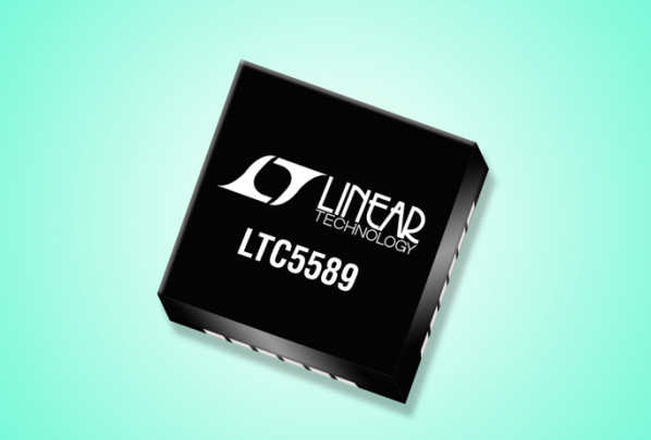
The LTC5589 supports not only narrowband but also wideband transmitters. Its baseband bandwidth extends up to 92 MHz with ±1 dB gain flatness, and it provides 184 MHz RF bandwidth at 1.8 GHz. Combining low power consumption and robust performance, this device is suitable for a wide range of demanding applications for radio and wireless communications.
These products include broadband modems, femto and picocell broadband wireless access, wireless microphones and portable audio systems, broadband portable field radios, unlicensed band radios, train communication, software-defined radios (SDR), portable RF test equipment, low-power microwave backhaul and repeaters, telemetry radios and satellite modems, etc.
Previous zero-IF modulators suffered from excessive carrier leakage and degraded sideband suppression, resulting in poor Error Vector Magnitude (EVM) and Adjacent Channel Power Ratio (ACPR) values. Calibration is a tricky process that relies on a digital tuning algorithm in a bandwidth FPGA using an external DAC.
Tuning resolution is generally limited. The LTC5589 provides on-chip tuning capabilities for I-channel and Q-channel phase and amplitude mismatches, affecting sideband suppression. This device also offers DC offset balance adjustment, which affects carrier leakage. With built-in controlled calibration capabilities via a serial port, the LTC5589 simplifies calibration tasks and enables cost-effective implementation.
The gain of the LTC5589 can be set via the on-chip serial port. The coarse gain control is 1 dB/step, and an adjustable fine gain control of 0.1 dB is also provided. The total gain range is –19 dB to 0 dB. If the modulator gain value fluctuates, it can affect the device supply current from 9mA to 39mA, and the device can be configured for lower power consumption with slightly reduced gain and performance depending on the requirements of a specific application. Once configured, the gain is automatically temperature-corrected by enabling the on-chip temperature correction function.
The LTC5589 is available in a 4mm x 4mm plastic QFN package and offers a small solution footprint. The operating temperature range is standardized to –40°C to 105°C. The device provides an enable pin for TDD or burst mode transmitter operation. When disabled, the LTC5589 conserves power by typically consuming 0.6μA of quiescent current. The modulator can be turned on at full quadrature accuracy within 350ns. The LTC5589 is priced at $4.45 per unit in 1,000-piece quantities and is available for mass production.

Comments
Related news
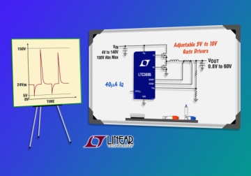
Linear Achieves Step-Down DC/DC Removal of External Surge Protection Devices
Linear Technology Korea (CEO Hong Sa-gwak) announced the launch of a high-voltage non-isolated synchronous step-down switching regulator controller using an external N-channel MOSFET (product name: LTC3895). The 4V to 140V (150V abs max) input voltage range is designed to operate with high input voltage sources or inputs with high voltage surge conditions, eliminating the need for external surge protection devices. LTC3895 ensures continuous operation at a maximum 100% duty cycle even as input voltage dips down to 4V, making it suitable for transportation, industrial control, robotics, and datacom applications.
2016.05.24by 명세환 기자
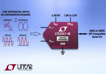
Linear, Analog Front End Circuit Simplified with SAR ADC Launch
Linear Technology Korea (CEO Hong Sa-gwak) announced the launch of a 16-bit 5Msps SAR (successive approximation register) ADC (analog-to-digital converter) (product name: LTC2311-16) that provides a wide rail-to-rail input common mode range. The LTC2311-16 features flexible differential inputs that accommodate analog signals up to the maximum Nyquist frequency. The product directly converts various signal types while providing excellent SNR (signal-to-noise ratio) of 81.6dB under 2.2MHz input signal conditions and achieving a high CMRR (common mode rejection ratio) of 85dB under the same high-speed input signal conditions.
2016.05.25by 명세환 기자
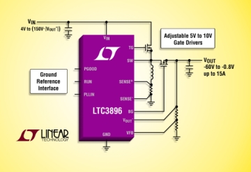
Linear Releases DC/DC Controller Using Single Inductor and Ground Reference Control
Linear Technology Korea (Representative Hong Sa-gwak) announced the release of a high-voltage inverting switching regulator controller (product name: LTC3896) that drives all N-channel synchronous MOSFET power stages. Most low-power or mid-level inverting DC/DC converters use coupled inductors or transformers. However, the LTC3896 uses only a single inductor and converts a positive input voltage of 4V to (150V − |VOUT|) into a regulated negative output voltage in the range of −60V to −0.8V at a maximum output current of 15 amperes. With maximum efficiency of 96%, it is ideal for transportation, industrial, telecom, and power distribution applications.
2016.05.26by 명세환 기자

Intel Unveils Next-Generation 'Core Ultra Series 3' and vPro Platform for Enterprise PCs
Intel has officially unveiled the "Intel Core Ultra Series 3" for next-generation enterprise PCs and the latest vPro platform, addressing a wide range of demands from enterprise notebooks to high-performance workstations.
2026.03.26by 배종인 기자

ROHM Launches ESD Protection Diode Compatible with High-Speed Interfaces of 10Gbps or Higher
Semiconductor specialist ROHM has developed the 'RESDxVx series' of ESD (electrostatic discharge) protection diodes capable of responding to next-generation high-speed data communication environments exceeding 10Gbps, simultaneously enhancing both signal quality maintenance required in high-speed interfaces and IC protection performance.
2026.03.26by 배종인 기자











