


Samsung Electronics Begins Full-Scale Mass Production of '2nd Generation 8GB HBM2 DRAM' with Maximum Transfer Capacity
 Published2018.01.11 12:11
Samsung Electronics is mass-producing the world's largest transfer capacity '2nd generation 8GB HBM2 (High Bandwidth Memory) DRAM' Aquabolt.
The 1.2V-based 2.4Gbps 2nd generation 8GB HBM2 DRAM 'Aquabolt' can process 307GB of data in one second, equivalent to 61 Full HD movies (5GB each), making it 9.6 times faster than the 32GB per second data transfer rate of existing high-performance graphics DRAM (8Gb GDDR5, 8Gbps).
In particular, if four 2.4Gbps 8GB packages are installed in a system, it can process up to 1.2TB of data per second, which can improve performance by up to 50% compared to 0.82TB of existing 1.6Gbps-based systems.
Samsung Electronics has branded this second-generation HBM2 DRAM product as "Aquabolt," a combination of "Aqua," which is indispensable for human survival, and "Bolt," which means fast as lightning.
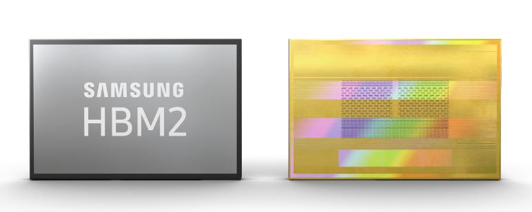
Through this mass production, Samsung Electronics plans to expand the premium HBM2 DRAM market, including supercomputers (HPC) and graphics cards, by more than three times compared to the existing market by supplying HBM2 DRAM exclusively in the industry, ranging from the first-generation 2.0/1.6Gbps 8GB HBM2 DRAM 'Flarebolt' to the second-generation 2.4Gbps 8GB HBM2 DRAM 'Aquabolt'.
The 2nd generation 8GB HBM2 DRAM 'Aquabolt' is a package that stacks 8 layers of 8Gb chips on a single buffer chip, and through the application of core technologies such as 'signal transmission optimization design' and 'thermal control,' it is the industry's first 2.4GbAchieved the operating speed of ps.
'Signal transmission optimization design technology' is a technology that minimizes the variation in signal transmission speed of each TSV pin, enabling HBM2 DRAM to maintain the highest level of performance, and 'thermal control technology' stably controlled the temperature of the chip by placing more thermal bumps between 8Gb HBM2 DRAM chips.
In addition, 'Aquabolt' adds a thin protective film to the bottom of the package to provide resistance to external shocks, enabling customers to improve productivity during the mass production process of systems.
"By being the only company in the industry to mass-produce the 2nd generation 8GB HBM2 DRAM, we have further strengthened our competitiveness as a product with a significant lead," said Han Jae-soo, Vice President of Strategy Marketing Team at Samsung Electronics' Memory Business Division. "We will continue to strengthen our unrivaled business capabilities in the premium DRAM market by establishing a stable supply system to meet the launch of next-generation systems by various customers."
Meanwhile, following the commencement of 'Aquabolt' supply to global IT customers, Samsung Electronics plans to lead the growth of the HBM2 DRAM market by further strengthening technological cooperation related to next-generation systems with supercomputer manufacturers, AI solution developers, and graphics companies.
Comments
Related news

Gartner: Global Semiconductor Revenue Surpasses $411.1 Billion in 2017
Gartner forecasted that the global semiconductor market revenue in 2017 would reach $411.1 billion, representing a 19.7% year-over-year increase. This marks the most pronounced revenue growth since 2010, which saw a 31.8% increase, reflecting recovery following the financial crisis. Jon Erensen, Principal Research Analyst at Gartner, stated, "Memory continues to drive semiconductor market growth, and due to supply-demand dynamics and resulting price increases, memory market revenue is projected to grow 57% in 2017. Memory shortages, particularly DRAM scarcity, are further driving up semiconductor revenue." He added, "This strong momentum is spreading to other semiconductor sectors including non-optical sensors, analog, discretes, and image sensors, which are expected to grow approximately 10% throughout 2017."
2017.10.16by 김지혜 기자
The CPU era is over, and the 'memory-centric computing' era is here
This year, memory has led the boom in the global semiconductor market. Memory experienced a surge because supply failed to keep up with demand, causing memory prices to rise. So what changes will the memory market face as the artificial intelligence (AI) era approaches? Doh Hyun-woo, senior research fellow at Mirae Asset Daewoo, stated: "We expect conditions to remain favorable through the first half of next year. DRAM will continue its upward price trend thanks to restrained capacity investment and server-type demand. NAND has started experiencing price increases due to iPhone X demand. Memory supply and demand are expected to remain balanced through the first half of 2018." He added: "In the fourth quarter of next year, Chinese memory semiconductor companies are scheduled to begin production on a small scale, which could be a variable factor." As memory semiconductor demand is expected to remain favorable, what issues should we pay attention to? The research fellow emphasized that memory-centric computing warrants close attention.
2017.10.23by 김지혜 기자
Samsung Electronics Begins Full-Scale Mass Production of '2nd Generation 10nm-Class (1y Nano) DRAM'
Samsung Electronics has overcome unprecedented process development challenges and is mass-producing "10-nanometer-class second-generation (1y nano) DRAM." Samsung Electronics has been mass-producing the world's smallest chip size 10-nanometer-class 8Gb DDR4 (Double Data Rate 4) DRAM since last month. Having initiated the full-scale 10-nanometer-class DRAM era by mass-producing "1x nano (10-nanometer-class first-generation) 8Gb DRAM" in February 2016, Samsung Electronics has overcome semiconductor process refinement limits in just 21 months.
2017.12.20by 김지혜 기자

Intel Unveils Next-Generation 'Core Ultra Series 3' and vPro Platform for Enterprise PCs
Intel has officially unveiled the "Intel Core Ultra Series 3" for next-generation enterprise PCs and the latest vPro platform, addressing a wide range of demands from enterprise notebooks to high-performance workstations.
2026.03.26by 배종인 기자

ROHM Launches ESD Protection Diode Compatible with High-Speed Interfaces of 10Gbps or Higher
Semiconductor specialist ROHM has developed the 'RESDxVx series' of ESD (electrostatic discharge) protection diodes capable of responding to next-generation high-speed data communication environments exceeding 10Gbps, simultaneously enhancing both signal quality maintenance required in high-speed interfaces and IC protection performance.
2026.03.26by 배종인 기자











