



Samsung Electronics Successfully Develops EUV-Based 5nm Foundry Process
 Published2019.04.17 17:00
| 25% area reduction and 20% power efficiency increase compared to 7nm
MPW Strengthens the Domestic Semiconductor Ecosystem Through SAFE
Samsung Electronics announced on the 16th that it has successfully developed a 5-nanometer process based on EUV (Extreme Ultra Violet) technology.

In addition, the company plans to ship 7nm products within this month and complete the design of 6nm products with the goal of mass production within this year.
Samsung Electronics' strategy is to strengthen its foundry technology leadership and the competitiveness of its system semiconductor business, which will lead the Fourth Industrial Revolution, by expanding its ultra-fine process portfolio.
Samsung Electronics' newly developed next-generation 5nm process reduces logic area by 25% compared to the existing 7nm process through cell design optimization, while also delivering 20% improved power efficiency and 10% improved performance. Furthermore, by leveraging design assets applied to the 7nm process, customers using the existing 7nm process can reduce design costs for the 5nm process.
Samsung Electronics is also fully ramping up mass production of its 7nm and 6nm foundry processes. Earlier this year, Samsung Electronics became the first in the industry to begin mass production of 7nm products using the EUV process, and plans to begin full-scale shipments this month. We are currently in production discussions with major customers for products based on the 6nm process, and the product design has been completed (tape-out) and mass production is scheduled for the second half of this year.
The EUV technology, which forms the basis of this ultra-fine process, utilizes an EUV light source with a shorter wavelength than conventional argon fluoride (ArF) light, enabling the creation of more detailed semiconductor circuits. This reduces the need for repeated multi-patterning processes, which involve engraving circuits, thereby improving performance and yield.
As Samsung Electronics secures core technology for advanced ultra-fine process foundry production, it is expected to strengthen the domestic system semiconductor ecosystem and enhance system semiconductor capabilities.
The foundry business has significant forward and backward linkages, as it requires the joint growth of various specialized companies in semiconductor equipment, materials, design, packaging, and testing.
Samsung Electronics plans to expand its 'MPW (Multi Project Wafer) Service', which produces multiple types of semiconductor products on a single wafer, to the latest 5nm process, allowing customers to more conveniently produce cutting-edge semiconductors.
In addition, through Samsung Electronics' foundry support program, 'SAFE (Samsung Advanced Foundry Ecosystem),' in addition to design assets, it provides design infrastructure to help design products based on the 5nm process, such as Process Design Kit (PDK), Design Methodologies (DM), and Electronic Design Automation (EDA). Fabless customers can use this to design products more easily and quickly, and bring new products to market sooner.
“Samsung Electronics’ EUV-based cutting-edge process has various strengths in performance and IP, and we expect high demand centered on new applications such as 5G, AI, and automotive,” said Bae Young-chang, Vice President of Strategic Marketing at Samsung Electronics’ Foundry Business Division. “We will continue to lead the future system semiconductor industry with our advanced process solutions.”

Samsung Electronics is producing cutting-edge EUV-based process products at its latest foundry production facility, the S3 line at its Hwaseong Campus, and plans to begin full-scale operation of the dedicated EUV line at its Hwaseong Campus, currently under construction, starting in 2020.
Comments
Related news
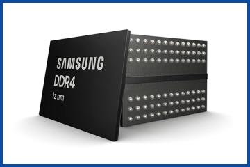
Samsung Electronics Develops World's First Third-Generation 10nm-Class DRAM
Samsung Electronics has developed third-generation 10-nanometer-class (1z) 8Gb DDR4 DRAM just 16 months after mass-producing second-generation 10-nanometer-class (1y) DRAM. The third-generation 10-nanometer-class (1z) DRAM improved productivity by more than 20% compared to the existing 10-nanometer-class (1y) DRAM without using expensive EUV equipment, and power efficiency was also enhanced through increased speed. Samsung Electronics has also completed approvals from major global CPU vendors in all evaluation categories for PC DDR4 modules based on third-generation 10-nanometer-class (1z) DRAM, enabling the company to significantly expand demand from global IT customers.
2019.03.21by 이수민 기자
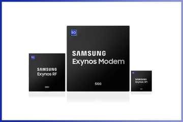
Samsung Electronics Launches Total Modem Solution to Reduce 5G Device Size
Modem chips, RF chips, and SM chips are core semiconductors for wireless communication technology that enable ultra-high-speed data communication. While modem chips convert voice and data information from mobile phones into signals or convert external signals into voice and data, RF chips adjust signals to enable transmission and reception of radio waves. In this process, SM chips adjust voltage to enable more efficient transmission of radio wave signals. Samsung Electronics has launched a 5G total modem solution by mass-producing the 'Exynos Modem 5100' along with the wireless frequency transceiver semiconductor 'Exynos RF 5500' and the power supply modulation semiconductor 'Exynos SM 5800'.
2019.04.04by 이수민 기자
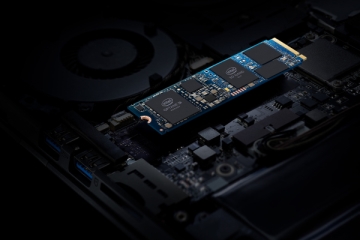
Intel Optane Memory H10 Solid-State Storage, a Memory and Storage Integration
Intel has announced the "Intel Optane Memory H10 with Solid State Storage," which combines the responsiveness of Intel Optane technology and storage capacity of Intel QLC (Quad Level Cell) 3D NAND technology in a single space-saving M.2 form factor. The Intel Optane Memory H10 with Solid State Storage enables Intel Optane Memory expansion even in space-constrained desktop form factors such as thin notebooks, all-in-one PCs, and mini PCs.
2019.04.13by 이수민 기자

Intel Unveils Next-Generation 'Core Ultra Series 3' and vPro Platform for Enterprise PCs
Intel has officially unveiled the "Intel Core Ultra Series 3" for next-generation enterprise PCs and the latest vPro platform, addressing a wide range of demands from enterprise notebooks to high-performance workstations.
2026.03.26by 배종인 기자

ROHM Launches ESD Protection Diode Compatible with High-Speed Interfaces of 10Gbps or Higher
Semiconductor specialist ROHM has developed the 'RESDxVx series' of ESD (electrostatic discharge) protection diodes capable of responding to next-generation high-speed data communication environments exceeding 10Gbps, simultaneously enhancing both signal quality maintenance required in high-speed interfaces and IC protection performance.
2026.03.26by 배종인 기자











