This page was machine-translated and may differ from the original. View original
Power supplies: The need for low-voltage, high-output implementation is growing.
ADI 3A 'LT3033' VLDO regulator connected in parallel
Increased output current to 3A or more, and heat dissipation is also possible.
Today's computing systems require more total power and lower supply voltages than in the past. Consequently, power supply designers must achieve high output current in a small space.
At low output voltages and high power densities, heat dissipation is a top design consideration, especially for linear regulators in low-noise applications. Connecting LDO regulators in parallel increases supply current capacity and reduces heat dissipation, lowering the temperature rise of specific components and reducing the size and number of required cooling devices.
Paralleling ADI's 3A LT3033 ultra-low voltage dropout (VLDO) regulators allows for applications requiring currents greater than 3A, while also dissipating heat. Furthermore, the LT3033's built-in output current monitoring function facilitates current balancing.
The LT3033 converts input power from 1.14 V to 10 V, delivering up to 3 A of load current and output voltages down to 0.2 V. The voltage dropout is only 95 mV at full load. Quiescent current is 1.8 mA during operation, dropping to 22 µA during shutdown. Programmable current limiting and thermal protection provide the robustness needed for high-current, low-voltage applications.
◇ 3A, Single VLDO Application Example
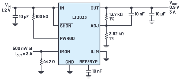
The LT3033, which supplies 3A at 0.9V from a 1.2V input, requires a minimum 10µF ESR ceramic capacitor on the IN/OUT pins for safety. Adding a forward-bias capacitor (CFF) between the VOUT and ADJ pins can improve transient response and reduce output voltage noise.

Using a 10nF bypass capacitor between the REF/BYP pin and GND typically reduces output voltage noise to 60µVrms over a bandwidth of 10Hz to 100kHz and provides a soft-start reference voltage. The minimum input voltage required for regulation is the greater of the regulated output voltage VOUT plus the dropout voltage or 1.14V.
The current limit is programmable by connecting a single resistor from the ILIM pin to GND and has an accuracy of ±12% over a wide temperature range. The external current limit can be overridden by the foldback internal current limit if the differential voltage between the input and output exceeds 5 V.

The LT3033 provides an output current monitor by driving the IMON pin to GND through a resistor. The IMON pin serves as the collector of a PNP, mirroring the LT3033 output PNP at a ratio of 1:2650. The resistance voltage is proportional to the output current as long as it is not higher than VOUT-400mV.
I OUT = 2650 × (V IMON / R IMON )
This output current monitor allows multiple LT3033 devices to share current. Despite its small size, the LT3033 incorporates several useful protection features, including foldback internal current limiting, thermal limiting, reverse current protection, and reverse battery polarity protection.
◇ Parallel connection of two LT3033s for 6A applications
Applications requiring more than 3A can be supported by paralleling multiple LT3033s.

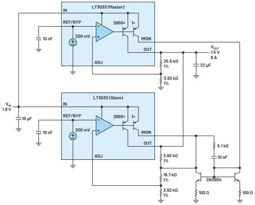
The figure above shows how two 2N3904 NPN devices and two LT3033s are connected in parallel to produce a 1.5 V, 6 A output. The individual IN and OUT pins are connected together. One master LT3033 controls the slave LT3033s.
The IMON pin is coupled with an NPN current mirror to create an amplifier. This amplifier injects current into the feedback divider of the slave LT3033, equalizing the IMON current of each LT3033.
The 100Ω resistor provides 113mV emitter degeneration at full load, ensuring excellent current mirror matching. The output voltage of the slave LT3033 is set to 1.35V, 10% lower than the circuit output, to ensure that the master LT3033 remains in control.
The feedback resistor of the slave LT3033 is sectioned to ensure adequate headroom for the slave NPN. A combination of a 10nF, 5.1kΩ capacitor and resistor added to the IMON pin of the slave device frequency compensates the feedback loop.
This circuit can supply a 6A load current, but current sharing accuracy is limited by the mismatch between the two NPN devices. This mismatch causes uneven heat distribution on the board. Replacing the two discrete NPN devices with a matched monolithic transistor, such as ADI's MAT14, allows for more accurate current sharing.
.jpg)
The MAT14 is a quad monolithic NPN transistor that provides high parametric matching, with a maximum current gain matching of 4%. Compared to the 2N3904, the MAT14 current mirror reduces current mismatch from 5.3% to 1.6%. The above compares the output current of an LDO regulator using discrete and matched NPN devices.
◇ Parallel connection of four LT3033s using matching components
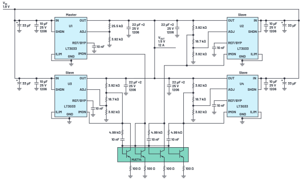
This parallel circuit architecture allows the current mirror to be expanded and the number of LT3033s to be expanded as needed by adding slave LT3033 devices.

The above is an example of 4 LT3033s connected in parallel using MAT14 for current sharing.

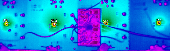
The above is thermal performance. Four LT3033s have a temperature range of 51 to 58°C. Considering the voltage drop along the input traces for each component, the solution appears to have even current sharing, as heat spreads evenly across the board.

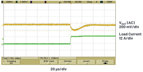
Above is the transient response of a 1.5V output, 12A power supply operating from a 1.8V input.
◇ LT3033, similar electrical efficiency to switching regulators
The LT3033 is a 3A VLDO regulator in a 3 × 4mm package. It features built-in output current monitoring and can be paralleled for high-current applications. With a voltage drop of only 95mV at full load, it is suitable for low input/output voltage, high-current applications, while achieving electrical efficiency comparable to switching regulators.
Additionally, it includes programmable current limiting, power good indication, and thermal limiting for a reliable and robust solution. Engineers developing battery-powered systems can achieve low standby current and reverse battery polarity protection.
This article is a summary of the article titled “Paralleling Very Low Dropout Linear Regulators for Increased Output Current and Even Heat Distribution” by Molly Zhu, Senior Applications Engineer, and Fei Guo, Field Applications Engineer, Analog Devices (ADI).
ADI 3A 'LT3033' VLDO regulator connected in parallel
Increased output current to 3A or more, and heat dissipation is also possible.
Today's computing systems require more total power and lower supply voltages than in the past. Consequently, power supply designers must achieve high output current in a small space.
At low output voltages and high power densities, heat dissipation is a top design consideration, especially for linear regulators in low-noise applications. Connecting LDO regulators in parallel increases supply current capacity and reduces heat dissipation, lowering the temperature rise of specific components and reducing the size and number of required cooling devices.
Paralleling ADI's 3A LT3033 ultra-low voltage dropout (VLDO) regulators allows for applications requiring currents greater than 3A, while also dissipating heat. Furthermore, the LT3033's built-in output current monitoring function facilitates current balancing.
The LT3033 converts input power from 1.14 V to 10 V, delivering up to 3 A of load current and output voltages down to 0.2 V. The voltage dropout is only 95 mV at full load. Quiescent current is 1.8 mA during operation, dropping to 22 µA during shutdown. Programmable current limiting and thermal protection provide the robustness needed for high-current, low-voltage applications.
◇ 3A, Single VLDO Application Example
The LT3033, which supplies 3A at 0.9V from a 1.2V input, requires a minimum 10µF ESR ceramic capacitor on the IN/OUT pins for safety. Adding a forward-bias capacitor (CFF) between the VOUT and ADJ pins can improve transient response and reduce output voltage noise.

▲ Typical LT3033 Application [Figure = ADI]
Using a 10nF bypass capacitor between the REF/BYP pin and GND typically reduces output voltage noise to 60µVrms over a bandwidth of 10Hz to 100kHz and provides a soft-start reference voltage. The minimum input voltage required for regulation is the greater of the regulated output voltage VOUT plus the dropout voltage or 1.14V.
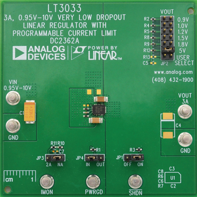
The current limit is programmable by connecting a single resistor from the ILIM pin to GND and has an accuracy of ±12% over a wide temperature range. The external current limit can be overridden by the foldback internal current limit if the differential voltage between the input and output exceeds 5 V.

▲ LT3033 demo board [Photo = ADI]
The LT3033 provides an output current monitor by driving the IMON pin to GND through a resistor. The IMON pin serves as the collector of a PNP, mirroring the LT3033 output PNP at a ratio of 1:2650. The resistance voltage is proportional to the output current as long as it is not higher than VOUT-400mV.
I OUT = 2650 × (V IMON / R IMON )
This output current monitor allows multiple LT3033 devices to share current. Despite its small size, the LT3033 incorporates several useful protection features, including foldback internal current limiting, thermal limiting, reverse current protection, and reverse battery polarity protection.
◇ Parallel connection of two LT3033s for 6A applications
Applications requiring more than 3A can be supported by paralleling multiple LT3033s.

▲ With two 2N3904 NPN devices
Two LT3033s connected in parallel [Figure = ADI]
The figure above shows how two 2N3904 NPN devices and two LT3033s are connected in parallel to produce a 1.5 V, 6 A output. The individual IN and OUT pins are connected together. One master LT3033 controls the slave LT3033s.
The IMON pin is coupled with an NPN current mirror to create an amplifier. This amplifier injects current into the feedback divider of the slave LT3033, equalizing the IMON current of each LT3033.
The 100Ω resistor provides 113mV emitter degeneration at full load, ensuring excellent current mirror matching. The output voltage of the slave LT3033 is set to 1.35V, 10% lower than the circuit output, to ensure that the master LT3033 remains in control.
The feedback resistor of the slave LT3033 is sectioned to ensure adequate headroom for the slave NPN. A combination of a 10nF, 5.1kΩ capacitor and resistor added to the IMON pin of the slave device frequency compensates the feedback loop.
This circuit can supply a 6A load current, but current sharing accuracy is limited by the mismatch between the two NPN devices. This mismatch causes uneven heat distribution on the board. Replacing the two discrete NPN devices with a matched monolithic transistor, such as ADI's MAT14, allows for more accurate current sharing.
.jpg)
▲ MAT14 matching monolithic quad transistor
Using parallel LDO regulators
Reduced shared mismatch [Figure = ADI]
Using parallel LDO regulators
Reduced shared mismatch [Figure = ADI]
The MAT14 is a quad monolithic NPN transistor that provides high parametric matching, with a maximum current gain matching of 4%. Compared to the 2N3904, the MAT14 current mirror reduces current mismatch from 5.3% to 1.6%. The above compares the output current of an LDO regulator using discrete and matched NPN devices.
◇ Parallel connection of four LT3033s using matching components
This parallel circuit architecture allows the current mirror to be expanded and the number of LT3033s to be expanded as needed by adding slave LT3033 devices.

▲ Four LT3033s connected in parallel with MAT14 [Image = ADI]
The above is an example of 4 LT3033s connected in parallel using MAT14 for current sharing.

▲ Thermal performance of four LT3033s connected in parallel [Photo = ADI]
The above is thermal performance. Four LT3033s have a temperature range of 51 to 58°C. Considering the voltage drop along the input traces for each component, the solution appears to have even current sharing, as heat spreads evenly across the board.

▲ Load transient response of four LT3033s connected in parallel [=ADI]
Above is the transient response of a 1.5V output, 12A power supply operating from a 1.8V input.
◇ LT3033, similar electrical efficiency to switching regulators
The LT3033 is a 3A VLDO regulator in a 3 × 4mm package. It features built-in output current monitoring and can be paralleled for high-current applications. With a voltage drop of only 95mV at full load, it is suitable for low input/output voltage, high-current applications, while achieving electrical efficiency comparable to switching regulators.
Additionally, it includes programmable current limiting, power good indication, and thermal limiting for a reliable and robust solution. Engineers developing battery-powered systems can achieve low standby current and reverse battery polarity protection.
This article is a summary of the article titled “Paralleling Very Low Dropout Linear Regulators for Increased Output Current and Even Heat Distribution” by Molly Zhu, Senior Applications Engineer, and Fei Guo, Field Applications Engineer, Analog Devices (ADI).
본 기사에 대한 정정·반론·추후보도 청구는 보도 청구 안내를, 그간 게재된 보도문은 정정·반론보도 모아보기를 참고해 주세요.