


UNIST's Department of Materials Science and Engineering Establishes Fundamental Theory of 2D Semiconductors
 Published2021.09.02 12:02
Presentation of a theory of substrate cross-section shapes favorable for synthesis
Helps in the synthesis of two-dimensional materials, including graphene
Two-dimensional new materials like graphene are synthesized on a metal substrate, using it as a "field." This process involves attaching vapor-state raw materials to the substrate to form a thin film. This method requires careful substrate selection, as substrate characteristics impact the quality of the two-dimensional material.
On the 2nd, a research team led by Professor Feng Ding of the Department of Materials Science and Engineering at Ulsan National Institute of Science and Technology (UNIST) theoretically presented criteria for selecting a substrate when synthesizing two-dimensional materials in the form of single crystals.
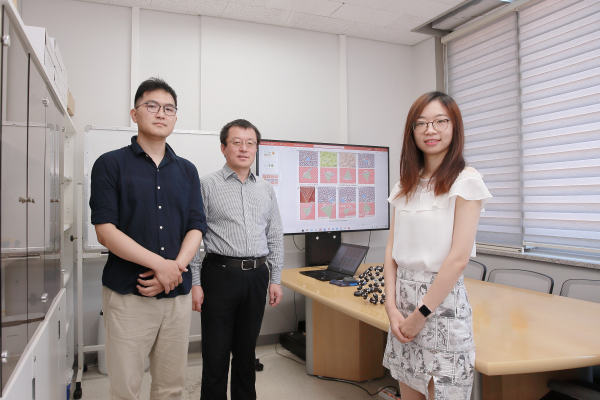
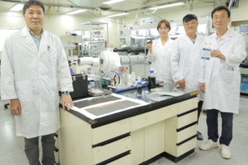
Researcher Pung Pung [Photo = UNIST]
Even for the same material, single-crystal forms are superior in quality to polycrystalline forms. Theoretical calculations suggest that high-Miller-index substrates, with their denser step-like structures across their cross-sections, are suitable for synthesizing two-dimensional materials in single-crystal form.
The Miller index is a mathematical representation of the cross-sectional shape of a material. Just as a watermelon has different cross-sectional shapes when cut lengthwise or cross-sectionally, a metal substrate like copper, with its atoms neatly arranged, also has different cross-sectional shapes depending on the cut direction. A high index surface, which is a diagonally cut cross-section, has a structure in which atoms are stacked one layer at a time like steps.
Professor Ding's research team previously discovered that high-Miller-index substrates are more suitable for synthesizing two-dimensional single-crystal materials than readily available low-Miller-index substrates. This time, they discovered that the denser the step-like structure, the easier it is to synthesize high-Miller-index substrates.
Contrary to theory, actual substrates are not perfectly flat and have uneven cross-sections. When the surface is uneven, the step edges are curved rather than straight. However, when the step structure is dense, the edge shape becomes closer to a straight line, which is advantageous for single crystal synthesis.
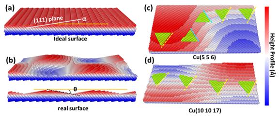
Whether single crystals can be synthesized by density [Figure = UNIST]
The research team discovered this by conducting computer simulations of synthesizing hexagonal boron nitride on high-Miller index copper substrates with various cross-sectional shapes. The simulation results also closely mirrored previous experimental results from two-dimensional material synthesis. “The results of this theoretical study demonstrate that high Miller index substrates should be actively utilized in the synthesis of two-dimensional single-crystal materials,” said first author Leining Zhang, a researcher.
Professor Fung Ding explained, “While the technology for synthesizing single-crystal silicon used in semiconductors has been studied for decades and a clear manufacturing method has been established, the technology for synthesizing newly emerged two-dimensional materials such as graphene and hexagonal boron nitride in single-crystal form is still in the early stages of research.”
He continued, “With the help of theoretical research that reduces the trial and error required to establish manufacturing technology for single-crystal two-dimensional materials, we expect to be able to develop technology to synthesize single-crystal two-dimensional materials in large quantities at a commercial level within 5 to 10 years.”
Two-dimensional materials are flat, flat materials just one atom thick. Representative examples include graphene, which is stronger than steel but also bends easily, and hexagonal boron nitride, which is gaining attention as a semiconductor insulator. The process of synthesizing two-dimensional materials as described above is called epitaxial synthesis.
This process involves three stages: first, the creation of crystal seeds; then, the growth of these single crystal seeds into small crystal fragments; and finally, the growth of these crystal islands, which then meet to form a single crystal. Polycrystalline materials are formed when the crystal islands grow in different directions.
The research was supported by the Institute for Basic Science (IBS), and the results were published on July 16 in the international academic journal Advanced Functional Materials.
Comments
Related news
Rediscovery of Graphene, the Next-Generation Foldable Quantum Dot Material!
A research team led by Professor Shin Hyun-seok at UNIST has for the first time discovered blue light emission at the interface between graphene and hexagonal boron nitride, known as 'white graphene'. Additionally, the team has successfully fabricated flexible light-emitting devices using 'graphene quantum dots', demonstrating graphene's potential as a novel display light source.
2020.10.27by 김동우 기자
Black phosphorus, could it become the main material for angstrom semiconductors smaller than nanometers?
The IBS Multidimensional Carbon Materials Research Group has realized a conductive channel with a linewidth of 0.43nm using two-dimensional black phosphorus. Two-dimensional black phosphorus is considered a leading semiconductor device for the post-graphene era. With a thickness of approximately one atomic layer, it can be applied to flexible and transparent devices that are difficult to implement with silicon-based semiconductors. Additionally, it exhibits the highest electron mobility among two-dimensional semiconductor devices.
2021.07.30by 이수민 기자
Korea Electrotechnology Research Institute transfers battery cathode material technology worth 1.1 billion won.
The Korea Electrotechnology Research Institute (KERI), a government-funded research institute under the National Research Council of Science and Technology within the Ministry of Science and ICT, has achieved a major milestone by developing mass production technology for a battery anode material that compensates for silicon's limitations with graphene, and successfully transferring the technology for 1.1 billion won.
2021.08.30by 배종인 기자

Intel Unveils Next-Generation 'Core Ultra Series 3' and vPro Platform for Enterprise PCs
Intel has officially unveiled the "Intel Core Ultra Series 3" for next-generation enterprise PCs and the latest vPro platform, addressing a wide range of demands from enterprise notebooks to high-performance workstations.
2026.03.26by 배종인 기자

ROHM Launches ESD Protection Diode Compatible with High-Speed Interfaces of 10Gbps or Higher
Semiconductor specialist ROHM has developed the 'RESDxVx series' of ESD (electrostatic discharge) protection diodes capable of responding to next-generation high-speed data communication environments exceeding 10Gbps, simultaneously enhancing both signal quality maintenance required in high-speed interfaces and IC protection performance.
2026.03.26by 배종인 기자











