



[Series] ST Engineer Yuji Kawano ⑮ – “MCUs with Built-in Oscillators, Device Characteristic Matching Is Essential”
 Published2022.03.08 10:55
MCU·오실레이터 회로 설계, MCU 부품 내장 문제 결정
사용자 매뉴얼·카탈로그 참조, 제조업체 권장사항 확인
[편집자주]일반적으로 반도체라 하면 컴퓨터의 CPU와 메모리처럼 일반인에게 익숙한 반도체를 떠올리기 마련이다. 반면에 전자제품 구동을 위해서 핵심 반도체로 쓰이는 MCU(Micro Controller Unit)의 경우 일반적으로 우리가 쉽게 접하는 모든 전자제품에서 사용되고 있으면서도 일반인에게는 아직 낯선 반도체다. 이런 MCU가 최근 반도체 부족 사태로 인해 언론에 오르내리며, 일반인들에게 주목받기 시작했다. 이에 본지는 MCU 반도체 전문기업인 ST마이크로일렉트로닉스의 유지 카와노 매니저의 연재기고를 통해 MCU에 대해 전문적으로 알아보는 자리를 마련했다.
 매우 정밀한 주파수를 생성하는 클록 생성기가 필요하다. 어떻게 크리스털 또는 세라믹 발진 소자를 MCU에 연결하는 오실레이터 회로를 설계할 수 있는가?
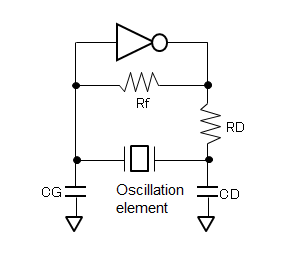
MCU 오실레이터 회로는 일반적으로 인버터를 사용한다. 발진을 유도하기 위해서 크리스털 또는 세라믹 발진 소자를 인버터에 연결한다. 오실레이터 회로의 기본적인 구성을 그림 1에 제시했다.
Rf : 피드백 저항. 이 저항이 발진을 안정화시킨다.
RD : 전류 제한 저항(Current restriction resistor). 이 저항은 전류를 제한하여 인버터가 크리스털 또는 세라믹 발진 소자를 과도하게 구동하지 않도록 해준다.
CG 및 CD : 부하 커패시터
이들 부품에 대한 명칭과 심볼은 그 제조업체에 따라 매우 다양하기 때문에 상세한 사항은 관련 발진 소자 또는 MCU의 사용자 매뉴얼을 참조하기 바란다. 발진에 영향을 미치는 또 다른 요인은 인쇄 회로 기판(printed circuit board, PCB)의 기생 용량(parasitic capacitance)과 저항이다.
이들 부품(Rf, RD, 또는 둘 모두)을 MCU에 내장할 수도 있다. 우리는 사용자들이 사용자 매뉴얼에서 권장하는 회로에 근거하여 이들 내장 부품, PCB 기생 성분, 부하 커패시터의 파라미터를 결정할 것을 권고한다. 이렇게 함으로써 크리스털 또는 세라믹 발진 소자의 특성들을 일치시킬 수 있기 때문이다. 모든 불일치는 발진 고장의 원인이 될 수 있다.
▲그림1 : 오실레이터 회로의 기본 구성

■ 어떤 부품 MCU에 내장할지 MCU·오실레이터 회로 설계에 달려
다음은 오실레이터 회로의 기본 구성을 보여주고 있는 그림 1에 대한 보다 상세한 설명이다.
어떤 부품을 MCU에 내장할 것인가는 MCU와 오실레이터 회로 설계에 의해 결정된다. 다양한 가능성이 있는데, Rf와 RD 모두를 내장할 수도 있고 Rf는 내장하고 RD는 외부에 연결해야 할 수도 있으며, 혹은 그 반대의 경우일 수도 있고 Rf와 RD 모두를 내장하지 않을 수도 있다. 대부분의 경우, 부하 커패시터(CG 및 CD)는 MCU에 내장하지 않으며, 외부적으로 연결시키거나 내장 발진 소자(발진 소자 모듈)를 사용해야만 한다. 사실 이들 커패시터 및 저항과는 별도로 사용자 PCB의 기생 커패시터와 저항 역시 고려해야만 한다.
일단 주파수를 결정했다면, 적절한 크리스털 또는 세라믹 발진 소자를 선택한다. 다음으로 선택한 발진 소자에 대한 사용자 매뉴얼 또는 카탈로그를 참조하여 어떤 회로(및 상수)를 제조업체가 권장하는지를 확인해야 한다. 권장된 회로를 구성하기 위해서 위에 언급한 부품들에 대한 파라미터를 선택해야 한다. 이들 부품들의 일부가 MCU에 내장되었다면 저항 및 정전용량에 대한 값을 확인해야 한다.
부품 파라미터들이 발진 소자 특성과 일치하지 않으면, 비정상적인 발진 특성을 나타내거나 심지어 전혀 발진하지 않을 수 있다.
■ 실제 오실레이터 회로
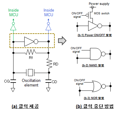
다음으로 실제 오실레이터 회로에 대해 살펴보자. 그림 2(a)는 MCU에 클럭을 제공하는 회로의 예를 나타낸 것이다. 여기에는 2개의 회로가 있다. 하나는 인버터의 입력 신호를 제공하고(녹색으로 표시), 다른 하나는 인버터의 출력 신호를 제공한다(청색으로 표시). 어떤 것을 선택해야 할지는 관련 MCU에 따라 달라지기 때문에 보다 자세한 정보는 MCU 사용자 매뉴얼을 참고해야 한다. 어떤 경우이든 발진 신호(클럭)는 먼저 입력 버퍼(예를 들어, 인버터)에 의해 파형으로 정형화되고 나서 MCU에 제공되어야 한다. 이것을 파형으로 정형화하면 입력 신호를 사인파(sine wave)로부터 MCU 내부에서 사용되는 것과 동일한 전압 수준을 갖는 직사각파(rectangular wave)로 변환한다.
▲그림2 : 실제 오실레이터 회의 다이어그램
그림 2(b)는 저전력 소모 모드와 같은 경우에 클럭 생성을 중단하는 3가지 방법을 보여준다. 그림 2(b-1)은 인버터에 전원을 차단하는 방법을 나타낸다. 그림 2(b-2)와 2(b-3)는 로직을 통해 클럭을 중단하는 방법을 설명한다. 그림 2(b-2)에서 인버터 대신 NAND 게이트를 사용하여 입력 신호를 L 레벨로 고정하고 출력 신호를 H 레벨로 유지한다. 그림 2(b-3)는 NOR 게이트를 사용하여 입력 신호를 H 레벨로 고정하고 출력 신호를 L 레벨로 유지한다. 최적의 방법은 여러분이 사용하고 있는 MCU에 따라 달라지기 때문에 보다 자세한 정보는 MCU 사용자 매뉴얼을 참조하기 바란다.
※ 주의
그림 2(b-1)에서 인버터 출력 단자는 높은 임피던스 특성을 갖기 때문에 전위(electric potential)가 불안정한 상태가 된다. 만약 중간 전위 수준을 가지고 있다면, 이것은 그림 2(a)의 입력 버퍼에 제공될 것이며, 심지어 회로가 저전력 소모 모드에 있는 경우에도 소모 전류를 예상했던 것보다 크게 유지하는 통과 전류(through current)를 생성하게 된다. 이와 같은 상황이 발생했다면, MCU 제조업체에 연락하여 해결 방안을 찾아야 한다. 그림 2(b-2)와 2(b-3)에 제시한 사례의 경우, 출력 레벨은 입력 버퍼에 제공하기 위해 H 또는 L로 유지되어 통과 전류의 발생을 방지할 수 있다.
■ 오실레이터 회로 배선은 가능한 짧게
오실레이터 회로는 노이즈 소스가 될 수 있으며, 외부 노이즈는 내부 클럭을 손상시켜 오류의 원인이 된다. 이용 가능한 다양한 MCU 회로 유형 중에서 오실레이터 회로는 노이즈에 가장 취약한 유형이다.
이 때문에 오실레이터 회로 배선은 가능한 짧게 해야 하고, 그 부품들(발진 소자, 커패시터, 저항)은 MCU에 가능한 한 가깝게 배치해야 한다.
▲그림3 : PCB 레이아웃
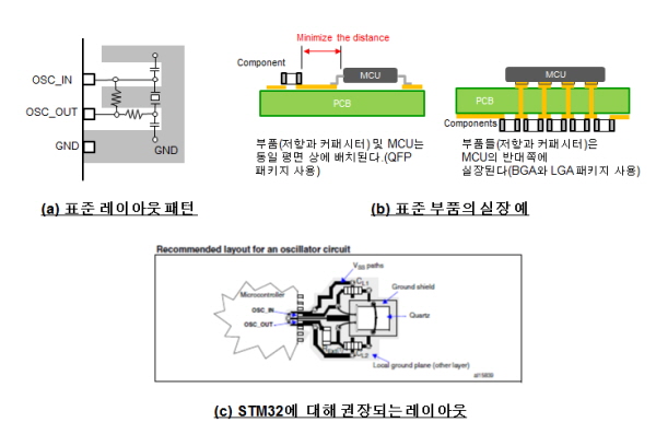
그림 3(a)은 오실레이터 회로에 가장 일반적으로 사용되는 레이아웃 패턴의 예를 제시한 것이다. 물론 여러분의 오실레이터 회로에 이러한 특정 패턴을 적용할 필요는 없다. 즉 여러분의 부품 크기와 형태에 따라 패턴을 설계할 수 있다. 그러나 다음의 규칙을 준수해야 한다.
(1) 부품들이 가능한 한 MCU에 가깝게 배치되어야 한다(그림 3(b) 참조).
(2) 배선은 가능한 짧게 해야 한다.
(3) 발진 소자를 접지-차폐(ground-shield)시키기 위해서 GND 패턴은 가능한 넓어야 한다. (※주의 : 일부 발진 소자들은 접지-차폐를 하지 않을 때 보다 양호한 노이즈-저항 특성을 갖는다. 이와 같은 경우, 사용자 매뉴얼을 참조하여 발진 소자를 조정해야 한다.)
(4) 이 회로와 다른 배선 사이의 누화를 방지해야 한다. (특히, 큰 전류 라인과 고속 신호 라인에 주의를 기울여야 한다.)
실제 예제로서 그림 3(c)은 ST마이크로일렉트로닉스의 STM32 MCU에 대해 권장되는 레이아웃 패턴을 보여주고 있다.
■ 오실레이터 회로 평가
오실레이터 회로는 다음 사항들을 감정함으로써 평가할 수 있다.
△부성 저항(negative Resistance, 이는 인버터 증폭 마진을 나타낸다) △고조파 성분 △발진 시작/정지 시 요구되는 전압 △발진 개시(안정화) 시간
이러한 평가 방법에 대한 상세한 설명은 발진 소자 제조업체의 웹사이트와 기술 노트에서 확인할 수 있다. 일부 제조업체들은 자사의 MCU에 대한 실제 결과와 발진 소자의 평가 내용을 웹사이트에 공개하고 있다. 이와 같은 정보들은 유용한 참고 자료로 활용할 수 있다.
발진 특성을 평가할 때 사용자에게 가장 중요한 것은 PCB의 기생 용량과 저항인데, 이들 파라미터가 오실레이터 회로에 포함되기 때문이다. 제조업체의 웹사이트에 게시된 평가 결과는 일반적인 회로에 대한 것이기 때문에 사용자 PCB의 회로 파라미터에 대한 데이터는 포함하고 있지 않다. 우리는 여러분이 자체 설계한 보드 상에 오실레이터 회로를 발진 소자 제조업체에 보내어 평가를 수행하도록 요청할 것을 권고한다. 대부분의 발진 소자 제조업체들은 이러한 요청을 기꺼이 수락한다.
기타 고려사항 및 참고 정보
(1) 오염된 PCB
과거에 한 고객이 발진 고장을 자주 경험한 후 회로 제조를 위한 생산 라인을 변경했다. 새로운 생산 라인에서 발진 고장의 원인이 적절하게 세척되지 않은 PCB에 있음이 밝혀졌다. 이것은 절연 저항을 감소시켜 발진 특성을 저하시키는 원인이 됐다. 수 메가 옴(ohm) 정도의 PCB 절연 저항은 발진 특성에 영향을 미친다.
(2) 발진 파형 증폭
최근 MCU 소비 전력이 감소함에 따라 MCU 오실레이터 회로 역시 더 적은 전력을 소모하도록 설계되고 있다. 전력 소비를 줄이는 한 가지 방법은 가능한 한 발진 증폭을 작게 하는 것이다. 이 방법은 발진 파형을 제어해 풀 스윙 대신 작은 증폭 특성을 갖게 한다.
(3) 발진 감지 회로
일부 최신 MCU 오실레이터 회로는 발진 안정성을 감지하는 회로를 포함하고 있다. 이 회로는 발진이 안정화되었음을 감지하면 플래그를 설정한다. 카운터가 일반적인 감지 방법으로 사용된다. 카운터는 클럭이 생성되기 전까지는 계수를 시작하지 않는다. 발진은 발진-감지 카운터의 출력 값을 판독함으로써 감지된다. 다른 방법은 클럭을 사용하여 내부 커패시터를 충전하는 것이다. 이 방법의 경우, 커패시터 전압이 일정해졌을 때를 감지하여 발진 클럭을 인식한다.

Comments
Related news

[Series] ST Yuji Engineer Kawano ⑫ - Timers, 'Pulse' Control via 'Clock' Calculation
MCUs are unfamiliar compared to CPUs or GPUs, yet they are among the most widely used semiconductors. Let's hear from Yuki Kawano, Manager of ST System Solutions Lab, about the vast utility and potential of MCUs.
2022.02.08by 명세환 기자

[Series] ST Engineer Yuji Kawano ⑬ – “RTOS Processing Completed Within Specified Time Range”
MCUs are unfamiliar compared to CPUs or GPUs, but they are among the most widely used semiconductors. Let us hear from Yuki Kawano, Manager of ST System Solutions Lab, about how great the utility and potential of MCUs are.
2022.02.15by 명세환 기자

[Serial] ST Yuji Kawano Engineer ⑭-“CISC·RISC, Selecting the MCU That Suits Your Needs”
MCUs are unfamiliar compared to CPUs or GPUs, but they are among the most widely used semiconductors. Let's hear from Yuji Kawano, Manager of ST System Solutions Lab, about how much utility and potential MCUs have.
2022.02.22by 명세환 기자

Intel Unveils Next-Generation 'Core Ultra Series 3' and vPro Platform for Enterprise PCs
Intel has officially unveiled the "Intel Core Ultra Series 3" for next-generation enterprise PCs and the latest vPro platform, addressing a wide range of demands from enterprise notebooks to high-performance workstations.
2026.03.26by 배종인 기자

ROHM Launches ESD Protection Diode Compatible with High-Speed Interfaces of 10Gbps or Higher
Semiconductor specialist ROHM has developed the 'RESDxVx series' of ESD (electrostatic discharge) protection diodes capable of responding to next-generation high-speed data communication environments exceeding 10Gbps, simultaneously enhancing both signal quality maintenance required in high-speed interfaces and IC protection performance.
2026.03.26by 배종인 기자











