


"Materials and equipment capabilities are essential to overcome the limitations of semiconductors."
 Published2023.02.23 15:55
CMP 슬러리·BEOL LOW-K·Wet Chemical·MI 공정
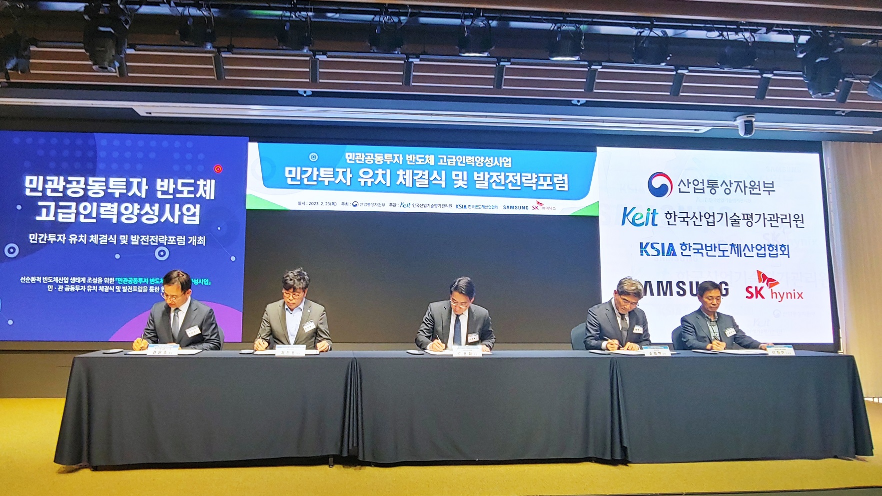
▲민·관 공동 투자유치 체결식 서명 모습

국내뿐 아니라 전세계적으로 반도체 인력난이 심화되고 있는 추세이다. 첨단산업 경쟁력 확보를 위한 국내 반도체 고급인력양성에 정부와 민간 함께 팔을 걷어붙이고 나선 가운데 차세대 반도체 개발의 한계돌파를 위한 기술 아젠다를 삼성전자·SK하이닉스가 공유하며 소재·인프라 공급망의 역할 중요성이 강조됐다.
산업통상자원부가 주최한 23일 반도체 고급인력양성을 위한 민·관 공동 투자유치 체결식과 발전전략포럼이 서울 논현동 보코서울강남에서 열렸다.
한국산업기술평가관리원·한국반도체산업협회·삼성전자·SK하이닉스가 주관한 이번 행사는 국내 반도체 산학연 관계자들이 모여 선순환적 반도체산업 생태계 조성을 위한 협력 강화를 모색하는 자리를 가졌다.
■ 정부·기업 ‘반반’ 투자로 반도체고급인력 강화
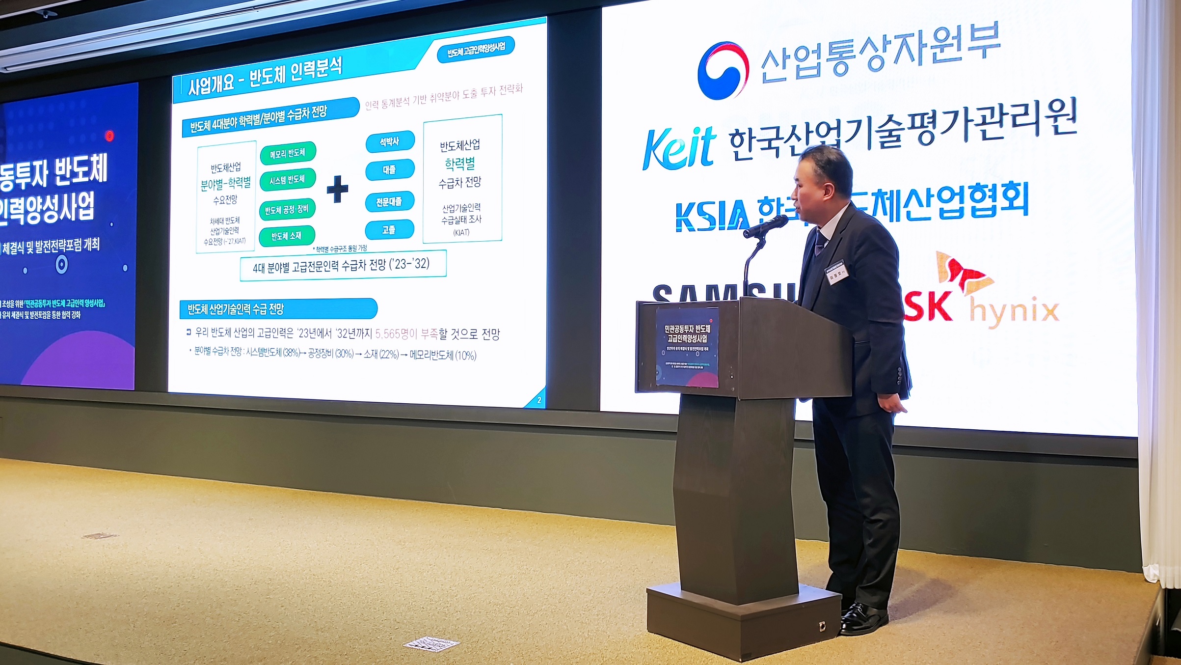
▲이정호 한국산업기술평가관리원(KEIT) 공정장비 PD
이용필 산업통상자원부 첨단산업정책과 국장은 개회사에서 “반도체 산업 발전을 위한 관건은 우수한 인재에 있으며 우수 인재 확보 전쟁 치열해지고 있다”며 급증하는 우수 인력 수요 대비 배출 인력의 절대적 부족을 꼬집었다.
그는 “대학의 반도체 커리큘럼과 시설 구축이 미흡해 민관협력 강화를 모색하며 2032년까지 2,228억의 투자액을 정부와 민간기업이 각각 50%씩 투자해 2,300여명의 반도체전문 석박사 인력 양성에 힘쓰겠다”고 밝혔다.
정부는 2032년까지 115개 연구개발 과제를 통해 4,388명의 석·박사 인력이 참여하고 2,365명의 고급전문인력 배출을 목표로 기업 실무형 고급인력양성사업을 추진한다.
이정호 한국산업기술평가관리원 공정장비 PD는 “2013년부터 10년 간 민간이 720억을 투자하며 총 1,443억원 투자액으로 166개 연구개발을 수행했다”며 “삼성전자, SK하이닉스, 원익IPS와 함께 민·관 공동투자로 2023년 100억 4,600만원의 예산을 투입해 신규과제 47건(국제 공동과제 6건)을 추진할 예정이다”라고 밝혔다. 이를 통해 반도체 산업을 견인할 수 있는 고급인력을 양성할 것으로 보인다.
■ 발전전략포럼, 반도체 경기·기술 전망 망라
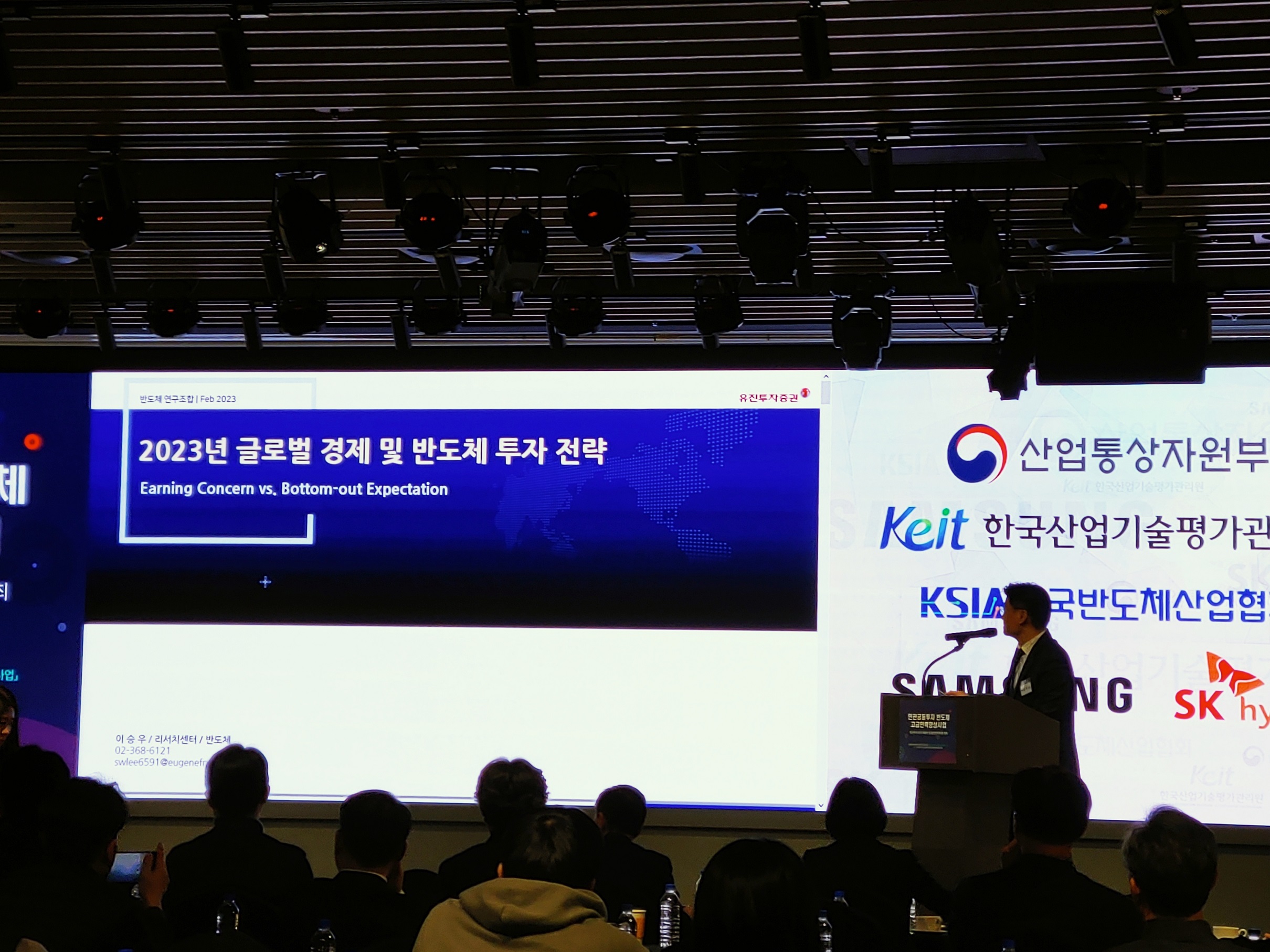
▲이승우 유진투자증권 센터장의 ‘2023년 글로벌 반도체 전망 및 투자 전략’ 세션 모습
이날 발전전략포럼에는 올해 반도체산업 경기 전망과 함께 △로직 디바이스 기술 △차세대 메모리 전망 △패키지 선도전략을 발표하며 반도체 산업 전체를 아울렀다.
이승우 유진투자증권 센터장의 ‘2023년 글로벌 반도체 전망 및 투자 전략’을 시작으로 △로직 디바이스 기술과 미래 준비(현상진 삼성전자 팀장) △차세대 메모리 반도체 기술전망(이성훈 SK하이닉스 부사장) △반도체 초격차 경쟁력을 위한 패키지 선도전략(김형준 차세대지능형반도체 사업단장) 세션이 진행됐다.
이승우 센터장은 “한국의 무역수지 적자폭이 확대됨에 따라 수출이 올해 하반기까지도 회복하기 쉽지 않을 것”이라고 전망하며 “반도체 산업을 끌어올리기 위해선 밸류에이션을 높이는 전략이 필요할 것”이라고 제언했다.
이 센터장은 “메모리 분야 강점을 가진 국내 반도체 산업은 재고가 과도할 뿐 아니라 생산 케파가 수요를 크게 상회해 감산은 선택이 아니다”며 현재 재고 적체 상황을 진단했다. 변수는 챗GPT의 흥행에 따른 사용자 트래픽 증가가 향후 서버 증설에 변수를 미칠지 추이를 주목하고 있다고 밝혔다.
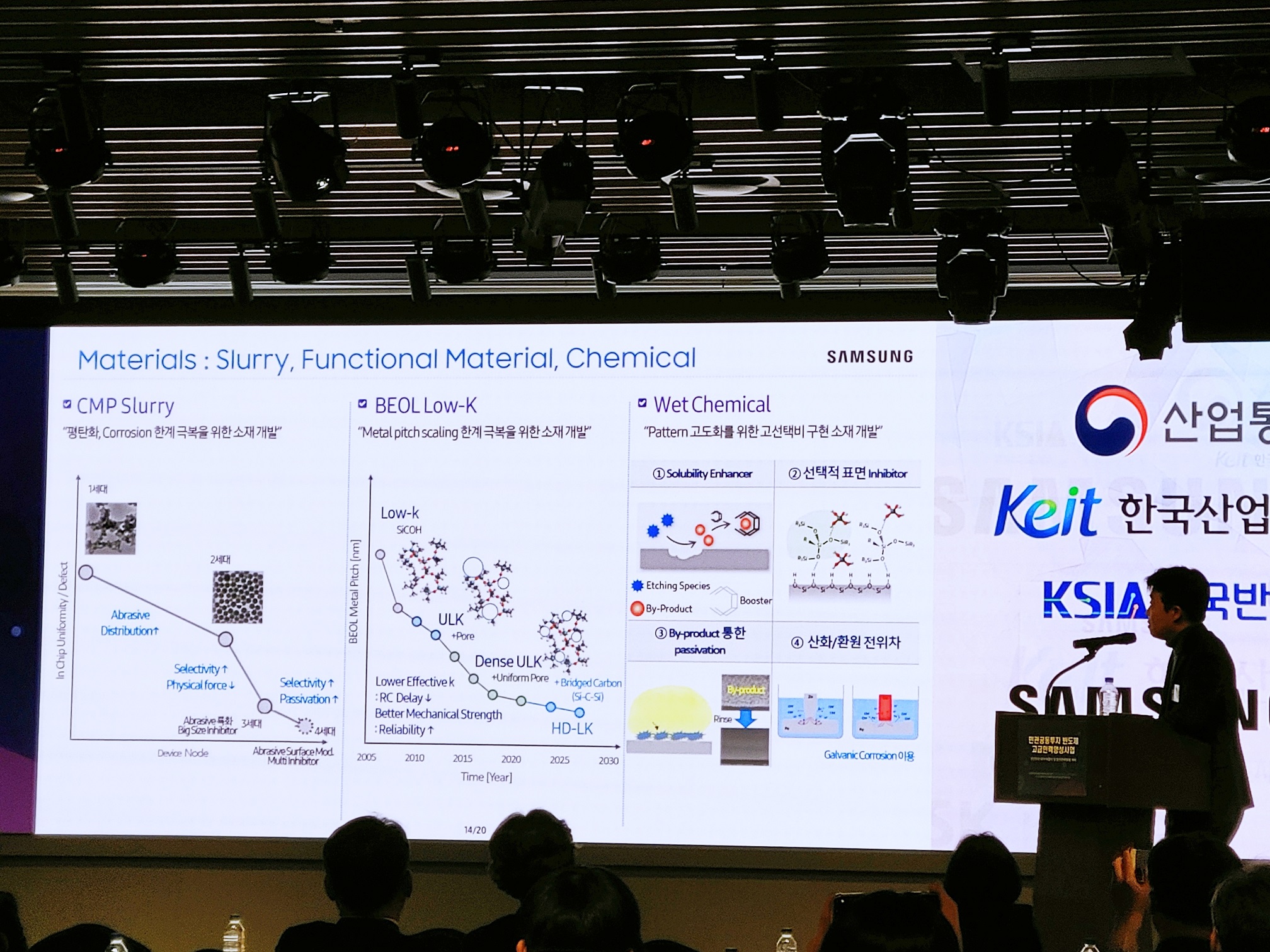
▲현상진 삼성전자 팀장 ‘한계돌파를 위한 로직 디바이스 기술' 발표
현상진 삼성전자 팀장은 ‘한계돌파를 위한 로직 디바이스 기술' 발표를 통해 “첨단 공정에서 가장 어려운 게 MOL(Middle of Line)”이라며 “MOL에서의 계면 저항, 게이트와 커넥트 사이 쇼트 등 난제들을 해결하기 위해 노력하고 있다”고 말했다.
차세대 반도체를 위한 난제들을 해결하기 위해선 소재 및 설비 역량이 점차 중요해지고 있다고 언급하며 ‘CMP 슬러리·BEOL LOW-K·Wet Chemical'의 발전 중요성을 강조했다. 이를 위해 협력 소재사 등과 함께 연구개발 중인 것으로 전해졌다. 또한 패터닝 프로세스에서 에칭의 중요성이 높아지고 있으며 드라이 클리닝 개발을 통해 파인 패터닝을 위해 노력 중이라고 밝혔다.
최근 계측 및 검사 공정이 반도체 9대 공정이라고 불릴 정도 중요해지고 있다는 현 팀장은 고분해능, 양산성을 고려한 측정 검사 속도 향상을 강조하기도 했다.

Comments
Related news

Intel Unveils Next-Generation 'Core Ultra Series 3' and vPro Platform for Enterprise PCs
Intel has officially unveiled the "Intel Core Ultra Series 3" for next-generation enterprise PCs and the latest vPro platform, addressing a wide range of demands from enterprise notebooks to high-performance workstations.
2026.03.26by 배종인 기자

ROHM Launches ESD Protection Diode Compatible with High-Speed Interfaces of 10Gbps or Higher
Semiconductor specialist ROHM has developed the 'RESDxVx series' of ESD (electrostatic discharge) protection diodes capable of responding to next-generation high-speed data communication environments exceeding 10Gbps, simultaneously enhancing both signal quality maintenance required in high-speed interfaces and IC protection performance.
2026.03.26by 배종인 기자

ST Launches 75V Drive IC Targeting 48V Industrial Motor Driving
ST Microelectronics has unveiled the 'STSPIN9P' series of 75V motor drive ICs tailored for 48V-class industrial drive system design. The new product family is characterized by half-bridge and full-bridge configurations that enable design scalability according to motor type and output conditions. Power supply circuits, protection functions, and current sensing circuits are integrated on-chip to simplify system configuration, and the devices are designed to support applications up to 500W maximum. The company plans to provide reference designs and demo boards to support development and evaluation in industrial automation, robotics, pumps, fans, lighting, and textile machinery.
2026.03.26by 배종인 기자

Nordic supports security updates for the entire lifecycle of IoT devices at a single fixed cost
Nordic Semiconductor, a global leader in low-power wireless connectivity solutions, has unveiled a single fixed-cost licensing model that delivers FOTA (Firmware Over-the-Air) and device management capabilities throughout the device lifecycle via nRF Cloud, and introduced a new firmware update solution to prepare for the enforcement of the European Union's Cyber Resilience Act (CRA).
2026.03.26by 배종인 기자
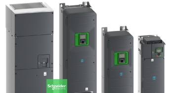
Schneider Aims for Building Energy Savings and Operational Stability with Next-Generation HVAC Drives
Schneider Electric has unveiled its next-generation HVAC drive product line 'Altivar HVAC'. The new product line's key features center on enhanced energy savings, system operational stability, and building management system integration. The products are divided into 'ATH200' for OEM and small equipment applications, and 'ATH600' for environments requiring continuous operation and advanced control. The company plans to expand the application scope from commercial buildings to facilities where HVAC system stability is critical, such as hospitals, airports, and data centers. The announcement includes over 30% energy savings, operation from -10°C to +60°C, Modbus and BACnet support, and compatibility with low global warming potential refrigerants.
2026.03.26by 명세환 기자











