



Applied Materials Invests Billions of Dollars in R&D Platform in Silicon Valley
 Published2023.05.24 09:46
▲Applied Materials EPIC Center
Dedicated Space in R&D Fab Available, Early Access to Next-Generation Processes and Equipment
Applied Materials is investing billions of dollars in an R&D platform that enables early access to next-generation processes and equipment for semiconductor innovation.
Applied Materials announced on the 22nd a groundbreaking investment in constructing the world's largest advanced semiconductor process technology and manufacturing equipment research and development (R&D) collaboration facility.
The new EPIC (Equipment and Process Innovation and Commercialization) Center is the heart of a rapid innovation platform designed to accelerate the development and commercialization of foundational technologies needed by the global semiconductor and computing industry.
Located on the Silicon Valley Applied Campus, this multibillion-dollar facility provides industry-leading capabilities and scale including over 180,000 square feet (equivalent to three American football fields) of state-of-the-art cleanrooms for collaborative innovation with chip manufacturers, universities, and ecosystem partners.
Designed to accelerate the pace of adopting new manufacturing innovations, the EPIC Center is expected to enable the industry to shorten the time required for technology to go from concept to commercialization by several years, while raising the commercial success rate of new innovations and the return on research and development investments across the entire semiconductor ecosystem.
Gary Dickerson, Chairman and CEO of Applied Materials, stated, "While semiconductors are more important to the global economy than ever, the technical challenges facing the industry are becoming more complex. This investment represents a golden opportunity to redesign how the global industry collaborates to provide the foundational semiconductor processes and manufacturing technologies needed to continue rapid improvements in energy efficiency and high-performance computing."
Applied's new EPIC Center is designed as the premier platform for leading logic and memory chip manufacturers to collaborate with the equipment ecosystem. For the first time, chip manufacturers can secure dedicated space within equipment suppliers' facilities to expand their internal pilot lines and gain early access to next-generation technologies and tools. This is possible months or even years before equivalent capabilities are installed at the chip manufacturers' own facilities.
The EPIC Center is expected to serve as a catalyst for accelerating the commercialization of academic research and strengthening the future semiconductor industry talent pipeline.
Universities have unparalleled capabilities in conceiving new concepts, but lack access to cutting-edge industrial laboratories and hardware, making it difficult to convert ideas into commercial reality. Applied's new platform provides university researchers access to the full range of industry-scale capabilities to validate their ideas, increasing innovation success rates and reducing the time and cost to commercialize new technologies.
Applied Materials will progressively invest a total of 4 billion dollars over the next seven years for establishing the EPIC Center. Completion is expected in early 2026, and it is anticipated to serve as a connection point for over 25 billion dollars in company R&D investments during the first 10 years of operation. The new center will employ up to 1,500 construction workers during the construction period in Silicon Valley and create up to 2,000 new engineering jobs, while potentially generating an additional 11,000 jobs in other industrial sectors. The EPIC Center is designed to potentially link with future U.S. National Semiconductor Technology Centers. Applied's investment scale may vary depending on U.S. government support through the Chips and Science Act provisions.

Comments
Related news

Intel Unveils Next-Generation 'Core Ultra Series 3' and vPro Platform for Enterprise PCs
Intel has officially unveiled the "Intel Core Ultra Series 3" for next-generation enterprise PCs and the latest vPro platform, addressing a wide range of demands from enterprise notebooks to high-performance workstations.
2026.03.26by 배종인 기자

ROHM Launches ESD Protection Diode Compatible with High-Speed Interfaces of 10Gbps or Higher
Semiconductor specialist ROHM has developed the 'RESDxVx series' of ESD (electrostatic discharge) protection diodes capable of responding to next-generation high-speed data communication environments exceeding 10Gbps, simultaneously enhancing both signal quality maintenance required in high-speed interfaces and IC protection performance.
2026.03.26by 배종인 기자

ST Launches 75V Drive IC Targeting 48V Industrial Motor Driving
ST Microelectronics has unveiled the 'STSPIN9P' series of 75V motor drive ICs tailored for 48V-class industrial drive system design. The new product family is characterized by half-bridge and full-bridge configurations that enable design scalability according to motor type and output conditions. Power supply circuits, protection functions, and current sensing circuits are integrated on-chip to simplify system configuration, and the devices are designed to support applications up to 500W maximum. The company plans to provide reference designs and demo boards to support development and evaluation in industrial automation, robotics, pumps, fans, lighting, and textile machinery.
2026.03.26by 배종인 기자

Nordic supports security updates for the entire lifecycle of IoT devices at a single fixed cost
Nordic Semiconductor, a global leader in low-power wireless connectivity solutions, has unveiled a single fixed-cost licensing model that delivers FOTA (Firmware Over-the-Air) and device management capabilities throughout the device lifecycle via nRF Cloud, and introduced a new firmware update solution to prepare for the enforcement of the European Union's Cyber Resilience Act (CRA).
2026.03.26by 배종인 기자
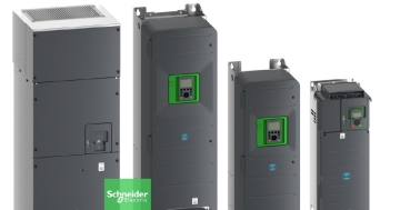
Schneider Aims for Building Energy Savings and Operational Stability with Next-Generation HVAC Drives
Schneider Electric has unveiled its next-generation HVAC drive product line 'Altivar HVAC'. The new product line's key features center on enhanced energy savings, system operational stability, and building management system integration. The products are divided into 'ATH200' for OEM and small equipment applications, and 'ATH600' for environments requiring continuous operation and advanced control. The company plans to expand the application scope from commercial buildings to facilities where HVAC system stability is critical, such as hospitals, airports, and data centers. The announcement includes over 30% energy savings, operation from -10°C to +60°C, Modbus and BACnet support, and compatibility with low global warming potential refrigerants.
2026.03.26by 명세환 기자











