



[Webinar Review] “Many Real-World Constraints on OP Amps… High EMI Immunity Offers Design Advantages”
 Published2023.11.20 14:36
▲ Lee Seong-jin, Researcher at ROHM
ROHM, Noise Evaluation Advantages with High EMI Immunity OP Amp
OP Amp, Caution regarding input offset voltage fluctuations due to stress
An ideal OP Amp can be imagined as having infinite input impedance, zero output impedance, infinite open-loop gain, no errors, and infinite voltage withstand capability, but in reality, OP Amps have various limitations.
Lee Seong-jin, a researcher at ROHM, said during the "OP Amp Introduction in 30 Minutes" webinar held at e4ds EEWebinar on the 14th, "To use real-world OP Amps perfectly, it is important to understand how various actual OP Amps differ and to select the optimal OP Amp and surrounding circuit constants."
Impedance refers to the amount of resistance in an AC circuit, and since the input impedance of an ideal OP Amp is infinite, no current flows from the input terminal to the OP Amp, nor is any current output. However, in the case of bipolar OP Amps, there are input impedances of hundreds of megaohms to several gigahertz (Ω), and for CMOS OP Amps, there are input impedances of tens of gigahertz to several terahertz.
The researcher emphasized that, as a point to note, the industry does not list input impedance values in datasheets, but instead lists them in the form of bias current.
It was suggested that, as the actual input impedance characteristics of an OP Amp are not infinite, attention should be paid to the bias current characteristics in the datasheet, and that a CMOS OP Amp should be used when connecting a sensor device with high output impedance to the OP Amp input terminal.
Furthermore, real-world OP Amps range from tens of milliohms to hundreds of milliohms; importantly, since output impedance changes significantly depending on the output voltage, the output impedance item is not listed in datasheets. Consequently, it is difficult to determine whether there are any issues with using the set based on the output impedance.
The researcher added, “To make a judgment, you must check the electrical characteristic graphs of output source current versus output voltage and output sink current versus output voltage in the datasheet.”
In addition, the input offset voltage occurs because the threshold voltage required to flow the same current does not perfectly match due to manufacturing variations of the transistors constituting the differential pair. These minute threshold voltage differences cause input offset voltage and are also affected by stress from the package and substrate.
The researcher cited fluctuations in input offset voltage caused by stress as a factor to watch out for regarding deviations in input offset voltage.
The researcher pointed out, “While market demands for noise immunity are becoming stricter every year, some IC makers are worsening noise immunity by pursuing a policy of integration into finer processes.”
ROHM announced the market launch of its EMARMOUR products, introducing high EMI immunity OP Amps that achieve noise immunity in radio wave radiation tests, BCI tests, proximity immunity tests, and DPI tests. The company emphasized that this provides the benefits of reducing the noise design load and decreasing the number of RC components.
The researcher stated, “ROHM’s OP Amps differentiate their noise characteristics, pursuing OP Amps that ‘do not generate noise and are unaffected by noise.’”
In addition to this, ROHM’s 30-Minute Introduction to OP Amp Webinar, you can also review ROHM EMARMOUR OP Amp at the e4ds EEWebinar, along with OP Amp principles, datasheet configuration and parameters, input offset voltage, and noise characteristics.

Comments
Related news
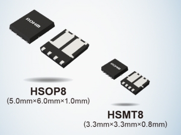
ROHM, 5 new products with industry's lowest ON resistance and low power MOSFETs
Rohm has developed a dual MOSFET with two 100V withstand voltage MOSFETs optimized for fan motor driving in telecommunications base stations and industrial equipment, mounting 2 chips in a single package, and has newly equipped five models: the 'HP8KEx / HT8KEx (Nch+Nch) series' and 'HP8MEx (Nch+Pch) series'.
2023.08.04by 배종인 기자

ROHM Wins Continental 'Supplier of the Year Award'
Rohm received the '2022 Supplier of the Year' award from Continental.
2023.08.10by 배종인 기자
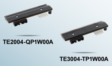
ROHM, Industry's Fastest 500㎜/s Printing Speed Thermal Print Head
Rohm has developed high-speed, high-reliability thermal print heads 'TE2004-QP1W00A (203dpi)' and 'TE3004-TP1W00A (300dpi)' optimized for barcode label printers used in label printing for logistics and inventory management.
2023.09.01by 배종인 기자

ROHM Develops Ultra-High Speed Gate Driver IC to Maximize GaN Device Performance
Rohm has started mass production of the gate driver IC 'BD2311NVX-LB' that drives GaN devices at ultra-high speed.
2023.09.21by 배종인 기자

ROHM Strengthens Analog IC Production Capacity
ROHM has strengthened its production capacity for analog ICs, centered on insulated gate driver ICs with expanding demand, through a new production building constructed at ROHM-Wako Electronics (Malaysia) Sdn. Bhd., its manufacturing subsidiary in Malaysia.
2023.10.17by 배종인 기자











