



Lam Research Fosters Semiconductor Process Design Talent
 Published2026.05.11 15:10
Lam Research is expanding the scope of domestic semiconductor talent development through a collaborative model involving industry, research institutions, and public organizations. Amidst increasing semiconductor process complexity, the company plans to cultivate industry-tailored talent through hands-on training utilizing virtual process environments.
Lam Research announced on the 11th that it is launching a training program for semiconductor process integration experts in cooperation with the Korea Semiconductor Industry Association (KSIA) and the Korea Institute for Industrial Technology Advancement (KIAT). This program is a collaborative talent development model based on industry-research-government linkages, aiming to strengthen the mid-to-long-term competitiveness of the domestic semiconductor industry.
This training course is an expansion of the collaborative program that Lam Research has been conducting with Sungkyunkwan University. Lam Research provides learning based on a virtual process environment by utilizing its simulation and modeling platform, 'Semiverse Solutions.' This platform virtually recreates advanced semiconductor equipment and process environments, enabling an understanding of the entire process and hands-on experience that is difficult to access in actual educational settings due to constraints.
In particular, it is explained that the program is structured to allow participants to directly perform process analysis and optimization in a virtual process design twin environment centered on 'SEMulator3D,' thereby enhancing the educational effect by linking theory and practice.
With the recent miniaturization and structural advancement of semiconductor processes, the importance of design capabilities that integrate and optimize the entire process flow, going beyond individual processes, is growing. This course reflects these industry demands and focuses on deepening the understanding of the overall process.
The target audience for the training consists of unemployed and employed individuals with basic process capabilities who wish to work in the semiconductor field. The program is operated at least three times a year and aims to train approximately 100 specialized personnel in the first year.
Lam Research stated that this program goes beyond single-company-centered education and represents a collaborative model in which industry, research institutes, and public organizations participate based on their respective expertise. Through this, the company plans to establish a talent development system to support the sustainable growth of the domestic semiconductor industry.
Park Jun-hong, General Manager of Lam Research Korea, said, “The demand for advanced process design talent that can be immediately utilized in the field is rapidly increasing,” adding, “We will establish a foundation for practical talent development through a collaborative model involving industry, research, and the public sector.”
Ahn Ki-hyun, Executive Director of the Korea Semiconductor Industry Association, stated, “This is an example of implementing a talent development model that meets industrial demands through the joint participation of global companies and public institutions,” adding, “We will continue our efforts to secure the future competitiveness of the semiconductor industry.”

Comments
Related news
Lam Research, Recruiting Intern with Full-time Employment Conversion
Lam Research Korea is recruiting interns in a permanent conversion track for the Field Service Engineer (Equipment Engineer) position. Application documents can be submitted through the Lam Research Korea recruitment homepage until January 15, 2025. Final intern candidates will be selected following document screening, interviews, and a health examination.
2025.01.02by 명세환 기자
Lam Research Korea, Full-time Field Process Engineer Recruitment
Lam Research Korea announced on the 24th that it is conducting recruitment for regular positions of Field Process Engineer.
2025.02.24by 명세환 기자
Lam Research Launches Advanced Packaging Equipment for the AI Era
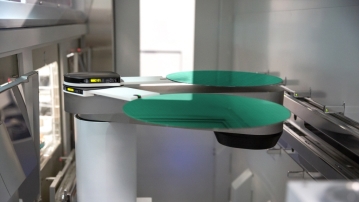
Global semiconductor equipment company Lam Research has launched VECTOR® TEOS 3D, an innovative deposition tool designed for the artificial intelligence (AI) and high-performance computing (HPC) era. VECTOR® TEOS 3D combines Lam Research's proprietary wafer bow management technology, dielectric deposition technology, and Equipment Intelligence® capabilities to achieve uniform inter-die gapfill up to 100 microns in thickness.
2025.09.11by 배종인 기자
“VECTOR® TEOS 3D Presents a New Paradigm for Advanced Packaging in the AI Era”
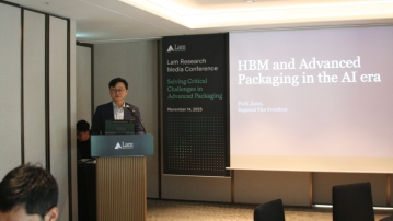
Lam Research is actively addressing innovative challenges in advanced packaging for the AI era through its 'Advanced Packaging VECTOR® TEOS 3D Portfolio'.
2025.11.14by 배종인 기자
Lam Research Manufacturing Korea is hiring semiconductor equipment manufacturing technicians on a large scale.
Lam Research Manufacturing Korea, the domestic subsidiary of Lam Research, a global leader in wafer manufacturing equipment, is recruiting new technicians to handle semiconductor equipment manufacturing operations.
2026.02.06by 명세환 기자











