


[CPU Planning ②] The goal is to expand the application of domestic cores in the field of autonomous vehicle image recognition
 Published2016.05.16 11:52
MENSA Core, IoT Field Expected… Application Expansion is Homework
[This is the second article following last week's feature, 'Domestic CPU Cores, How Much Do You Know?']
The Aldebaran CPU core is a core independently developed by the Electronics and Telecommunications Research Institute (ETRI). Its name comes from the name of the first-magnitude star representing the constellation Taurus. This processor integrates a CPU core based on a power-minimized microarchitecture and an ADE (Application Development Environment) including an open source (GNU)-based software toolchain for increased interoperability with enterprises.
Aldebaran's microarchitecture and CPU core design code (RTL) are ETRI's proprietary technologies, which companies can secure as their own technology through consultation, and not only can they develop additional functions requested by companies, but their technological uniqueness can also be protected by ETRI's intellectual property rights. The Aldebaran S2 SoC, an SoC utilizing the Aldebaran CPU core, was manufactured using TSMC's 65nm process and has a maximum operating speed of 800MHz and energy efficiency of 0.24mW/MHz, which is the best power efficiency in the industry, ETRI said.
Aldebaran is implemented with a deep pipelining (13-stage) structure, enabling high-speed execution at 800MHz@65nm (1GHz@45nm) and implementing a branch predictor to maximize performance. The Aldebaran CPU core is a 13-stage dual-issue superscalar architecture with branch prediction, instruction queue structure, and cache activation frequency minimization for power consumption minimization, DVFS, etc. This high-performance, low-power structure indicates that the Aldebaran CPU core is an architecture suitable for wearable smart devices.
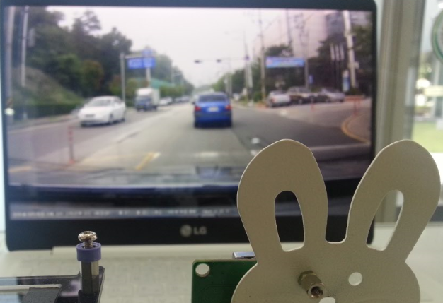
▲ Demonstration of the Aldebaran processor applied to the automotive image recognition field.
ETRI’s Intelligent Semiconductor Research Division stated, “The Aldebaran CPU core is a RISC core based on 32-bit instructions and data and has a 13-stage pipeline,” and “The CPU core is divided into three domains, and each domain has a structure that maximizes the operating frequency by implementing the instruction storage at the boundary of each domain to maximize performance.”
The Aldebaran CPU core has a GNU compiler and software ecosystem for increased interoperability, and the Linux kernel runs stably. In addition, there is a separate high-speed debugging module called “Aldebaran Eyes” inside the core, and data can be sent and received externally via the USB2JTAG interface (5 pins). Aldebaran Eyes is a minimal-footprint debugging module that provides a variety of features for software debugging, including Stop, Resume, Register probe/set, TLB probe/set, and memory probe/set for CPU cores.
ISO26262 Compliant 1GHz Aldebaran Processor Launched in April
For the application of the Aldebaran CPU core, various evaluation systems are provided, namely, the Aldebaran S2 SoC-based system, the Xilinx Virtex-7 2000T FPGA board-based system, and the Xilinx Artix-7 200T-based low-cost system. The Aldebaran S2, developed by ETRI using Aldebaran, includes the Aldebaran IP and includes the DVFS (Dynamic Voltage Frequency Scaling) function, so that it can be used in various power modes. In addition, the Aldebaran-TS3, developed by ETRI using the Aldebaran-FT, integrates four processor cores and performs functions such as video compression, synthesis, and sensing.
Currently, Aldebaran has developed ABCore-S2, S4, CL, and CT, and is developing ABCore-HoC, which implements Neural-Core deep learning that enables many-core-based human intelligence, and ABCore-NANO, which can be used in IoT, wearable devices, drones, etc. Aldebaran CPU cores have both technological and cost competitiveness, and can contribute to SoC technology for IoT, robotics, and automotive fields, and can replace embedded CPU cores that are currently being imported.
Researcher Kwon Young-soo of the Processor Research Lab at the Electronics and Telecommunications Research Institute said, “Aldebaran, which applies image recognition and ISO26262, can be used as an automotive safety processor,” and “In the automotive semiconductor field, which is mostly occupied by foreign companies, domestic companies are relatively focusing on image recognition technology, so our goal is to apply the Aldebaran processor to this.” In particular, the vehicle image recognition field has a bright future as it belongs to the core function of autonomous vehicles, which are expected to be an issue in the future. ISO26262, an automotive functional safety standard, prioritizes performance and safety and is also necessary for ADAS (Advanced Driver Assistance Systems).
Researcher Kwon continued, “The 1GHz Aldebaran processor compliant with ISO26262 was released in April,” and emphasized, “Based on this, the Aldebaran processor will apply ISO26262 to high-performance processors like global companies such as Renesas and Infineon, targeting the image recognition high-performance ADAS market.”
Unmanned Solutions “Military, ADAS Test, Drone, Agricultural Mobile Robot SoC Utilization”
Unmanned Solutions has developed an integrated SoC for mobile robot platform control using the Aldebaran processor.
The company carried out AMBA bus design and RTL design between the Aldebaran processor and each IP. In addition, we built a Xilinx Kintex FPGA test platform and an application board for performance testing of each Peri to test each design, and tested the I/F MDF implementation and performance between the mobile robot platform and the FPGA application.
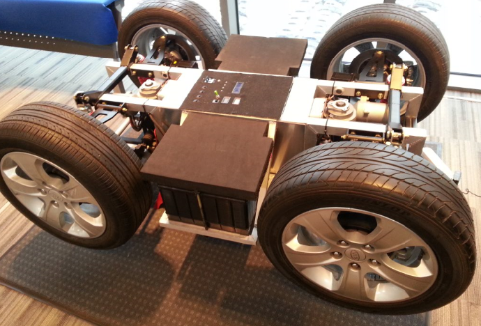
▲ A mobile device steering system created using the Aldebaran processor.
The Unmanned side stated that they received the SW toolchain including the Aldebaran RTL design environment and compiler from ETRI, the core holding organization, and were able to build a debugger and integrated development environment for Aldebaran. ETRI also supported Aldebaran RTOS porting, test kit and sample FPGA board support, and the Aldebaran visual platform. In particular, the company stated that they were able to acquire know-how in terms of cooperation, such as receiving support for small mobile robot platform SoC specifications and detailed design methods.
“AMBA Compatible made it easy to connect the Aldebaran core and peripherals, so we were able to easily design the bus architecture connection between each IP and the core,” said Woo Hoon-jae, head of the Unmanned Solution Lab. “The dual-score structure of the Aldebaran core made it easy to develop applications on multiple cores and processors.” Director Woo continued by citing the advantages of the integrated development debugger and integrated development environment for the Aldebaran core, including its ease of development and use, and its support for various OSs, including real-time OSes.
We need a variety of integrated development environments that can be used on general-purpose OSs.
In particular, he said that there are no multi-core MCUs among MCUs based on ARM Cortex M4/M7, and that the characteristics of general-purpose ARM core MCUs allow for customized designs compared to the number of fixed interfaces and unnecessary interfaces.
However, Director Woo pointed out that lower cycle calculation processing speed than existing FPUs is required for more complex algorithm processing speed, and various integrated development environments that can be used on general-purpose OSs are needed for a wide range of user development environments. He also hoped to build mutual connections with core organizations for device drivers and continuous FAQs on core performance improvement at the start of commercialization.
Based on this mobile robot SoC development, Unmanned sees high potential for use in the military, ADAS testing, drone testing, and especially in the agricultural field.
MENSA plans to build a development environment based on ECLIPSE
Although the performance of general-purpose CPUs and DSPs focusing on high-speed repetitive calculations is continuously improving, they have a structure that is not suitable for high-speed, large-capacity calculations for processing intelligent algorithms. Among the most widely used intelligent algorithms, neural networks, genetic algorithms, or brain-inspired algorithms have been reported to have various applications, but it is often difficult to implement practical systems due to limitations in computational amounts.
In other words, hardware-based MCU development that can efficiently compute intelligent algorithms is required as computational functions and learning capabilities that optimize given situations are required. To meet these requirements, the Electronics and Telecommunications Research Institute developed the MENSA core.
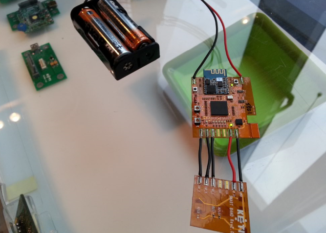
▲KET I implemented a low-power sensor system using the MENSA core.
The MENSA (Microcontroller with Enhanced Numeric, Scheduling and Artificial intelligence unit) core expands the structure of a lightweight MCU based on the Integer Unit by adding a scheduling function that enables multi-bus distributed operations to the functions of an extended bus and command decoder. It is designed to be able to freely expand and use the functions of NNPU (Neural Network Processor Unit), GAU (Genetic Algorithm Unit), and NPU (Neuromorphic Processor Unit) that can provide artificial intelligence functions as well as FPU, a high-speed computational element such as DSP. Through these functions, it can be used not only for lightweight platform design but also for configuring various distributed computational IoT platforms with intelligent functions.
The MENSA-based recognition algorithm processing SoC supports a search algorithm based on a genetic mechanism of natural selection, such as a non-learning-based genetic algorithm rather than a learning-based one. It also supports intelligent GAU operations to find coefficient values of PPCs of the third or higher order, and is a complex signal processing SoC capable of simultaneously correcting four or more complex sensor signals.
KETI, "Plans to expand to mobile, intelligent cars, IoT devices, drones, etc."
There is also a sensor signal processing SoC utilizing GAU using MENSA core. It defines 26 command sets and supports many kinds of neural network algorithms and image algorithms through this, and supports easy and flexible control and efficient 'error back propagation' algorithm by using a mixed use of Bus and Ring. It reduces the time to calculate non-linear values by designing NFU (Non-linear function Unit) using LUT (look-up table). Development of a voice SoC using MENSA is also in progress. We plan to build a verification platform using FPGA and support SoC Top design by providing simulation models.
Kim Dong-sun, a manager at the Electronics and Telecommunications Research Institute, said, “In the future, MENSA plans to build a development environment based on ECLIPSE,” and “Based on this, we plan to expand applications to mobile, intelligent automobiles, IoT devices, drones, and robots.”
Comments
Related news
Will domestic production of image processing processors secure competitiveness in autonomous vehicles?
The Aldebaran processor is a purely domestic Korean CPU that does not use ARM cores and is capable of supporting high-resolution video processing, offering bright prospects for the realization of autonomous vehicles in the future. The new Aldebaran processor, AB-TS3, is equipped with a quad-core capable of 4K video processing, an H.265 (HEVC) encoder, and VD/PD/LD engines.
2015.10.12by 신윤오 기자
[CPU Planning ①] How Much Do You Know About Domestic CPU Cores?
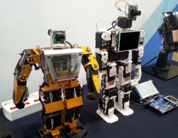
The domestic CPU core roadshow introduced Core-A from Dynarit Systems, emCore from A.D. Chips, Aldebaran from the Electronics and Telecommunications Research Institute (ETRI), and MENSA core from the Korea Electronics Technology Institute (KETI). SoC development cases utilizing these cores were demonstrated by participating companies, including Believe Micron's location-based wireless communication SoC for digital transceivers (applying Core-A), MCS Logic's wireless speaker SoC with embedded USB DAC (applying emCore), and Unmanned Solution's small mobile robot platform control SoC (applying Aldebaran).
2016.05.10by 신윤오 기자
[Reporter's Notebook] Will the application of domestic cores be a money-maker or a bomb?
AD Chips selected 'CPU' with high technical difficulty as a breakthrough for survival as a venture company in 1998. This was because at that time, there was no readily usable CPU (Central Processing Unit) core available domestically. The company believed that developing a CPU core, which is essential for SoC design, would create a competitive moat that even large corporations could not easily catch up to. Lee Hee, Vice President of AD Chips, stated, "As a person who studied electronics engineering, I chose CPU technology as a legacy to leave behind and as technology to pass on to future generations." However, the challenge was technology. In a situation where overseas companies possessed strong leading-edge technologies, the company needed to secure differentiation and competitiveness. It also had to avoid intellectual property disputes with companies such as ARM, Intel, and IBM. The technology that emerged from these efforts became EISC (Extended Instruction Set Code) ISA, which forms the foundation of Korea's homegrown CPU core, emCORE.
2016.05.10by 신윤오 기자
[e4ds Tech Day 2026 ⑨] Sim Sang-gyu, Autocrypt CTO: "In the Physical AI Era, Automotive Security Must Extend Beyond the Vehicle"
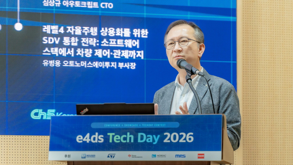
At e4ds Tech Day 2026, Sim Sang-gyu, CTO of Autocrypt, explained automotive cybersecurity strategies in the era of Physical AI and SDV (Software-Defined Vehicle). Automobiles are evolving as part of an ecosystem connected to AI, cloud, chargers, IoT, and robots, and he emphasized that the scope of security must expand beyond the vehicle interior to the entire connected environment. In particular, AI model tampering, adversarial attacks, OTA updates, and EV charger hacking were identified as major threats. He explained that response measures require zero trust, AI model integrity protection, intrusion detection, Security by Design and Default, and full lifecycle security management, and that proactive security system establishment beyond regulatory compliance is critical for securing future mobility competitiveness.
2026.10.12by 배종인 기자

Practical HIL Construction Strategy for Automotive and Off-Highway Controller Validation
As vehicle E/E architecture transitions to zonal structures and shifts to software-defined vehicles (SDV), the number of controllers (ECUs) requiring validation and software complexity are surging dramatically. Meanwhile, real vehicle testing cannot provide repeated verification under identical conditions and entails lead time and safety concerns. This white paper explains the principles of HIL (Hardware-in-the-Loop) validation and the structure of the NI platform composed of PXI, SLSC, and VeriStand, and through two actual implementation cases—Camera Record & Replay HIL for In-Cabin Monitoring Controller (ICMU) and Forklift Controller (VCU) HILS—describes how controller-level regression testing becomes possible. Additionally, it explicitly states application boundaries and limitations, such as lack of A2B support.
2026.10.12by 편집부











