



Samsung Electronics, Moving Beyond 14nm Process to Mass-Produce 10nm Logic, 'To be Incorporated into Products Early Next Year'
 Published2016.10.17 17:01
27% performance increase, 40% power consumption decrease, and 30% increase in chip production per wafer compared to 14nm
Samsung Electronics has secured cutting-edge process leadership in the system semiconductor field by starting mass production of the industry's first 10-nanometer logic process.
Following the industry's first mass production of 14nm mobile APs last January, Samsung Electronics is now the first in the entire system semiconductor industry to use the 10nm process
Mass production has begun.
The 10nm first-generation process, which has just started mass production, has improved performance by 27% and reduced power consumption by 40% compared to the existing 14nm first-generation process, and increased chip production per wafer by approximately 30%.
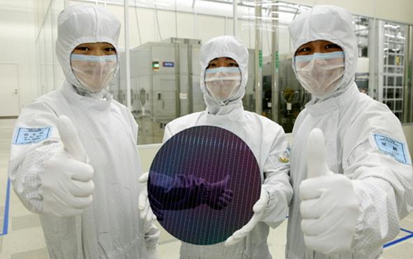
<Reference photo: Samsung Electronics employees showcasing semiconductor products>
Mass production of the 10-nanometer process requires patterning work to draw circuits that are much more precise and fine than those of the 14-nanometer process. Samsung Electronics has overcome the limitations of the micro-process and secured design flexibility by applying triple patterning technology, which repeats the patterning process three times using existing equipment.
Samsung Electronics has started mass production of the 10-nanometer first-generation (10LPE) process and is developing the second-generation (10LPP) process with improved performance, aiming for mass production in 2017. The company plans to utilize the 10-nanometer process for a long period through continuous performance improvements and the expansion of derivative processes beyond the second generation.
In addition, Samsung Electronics is expanding its foundry ecosystem by verifying design tools for the 10nm process through collaboration with customers and partners, and by providing product-level design kits and IP design kits to help customers develop products.
"With the mass production of the 10nm logic process, we have once again proven that Samsung Electronics' micro-process technology is at the industry's highest level," said Yoon Jong-sik, Vice President and Head of the Foundry Business Team at Samsung Electronics' S.LSI Division. "Going forward, we will continue to advance our system semiconductor business by securing micro-process technology through continuous technological innovation and providing differentiated semiconductor solutions to our customers."
Products utilizing Samsung Electronics' 10nm logic process are set to expand to various customers and products, starting with the installation of new IT products to be released early next year.
Comments
Related news
Samsung Electronics Unveils 'Exynos 8 Octa,' a 14nm Process-Based One-Chip Solution
Samsung Electronics has unveiled the "Exynos 8 Octa (8890)," a premium-class second-generation mobile SoC that applies state-of-the-art 14-nanometer FinFET process technology. The "Exynos 7 Octa," the first-generation 14-nanometer product that began mass production for the first time globally earlier this year, is a standalone mobile Application Processor (AP), whereas the second-generation product announced this time is characterized by integrating a mobile AP and a top-tier modem into a single chip.
2015.11.12by 신윤오 기자

AMD Unveils 14nm FinFET Process-Based GPU Architecture
AMD unveiled a new Polaris GPU architecture at CES 2016. The company stated that this new architecture, based on significantly improved design, delivers high performance per watt and incorporates the latest features such as HDR monitor support. AMD anticipates that it will be able to ship GPU products based on the Polaris architecture starting from mid-2016.
2016.01.05by
Samsung Electronics Mass-produces Longer-lasting Wearable APs Using '14nm FinFET'
Samsung Electronics announced mass production of 'Exynos 7270,' a wearable-dedicated AP (application processor) that applies 14-nanometer FinFET process technology. Following the expansion of 14-nanometer advanced process, which delivers high performance and low power consumption applied to premium mobile APs, to the budget segment in early this year, Samsung Electronics has now applied this technology to a wearable-dedicated AP for the first time in the industry.
2016.10.12by 신윤오 기자

Intel Unveils Next-Generation 'Core Ultra Series 3' and vPro Platform for Enterprise PCs
Intel has officially unveiled the "Intel Core Ultra Series 3" for next-generation enterprise PCs and the latest vPro platform, addressing a wide range of demands from enterprise notebooks to high-performance workstations.
2026.03.26by 배종인 기자

ROHM Launches ESD Protection Diode Compatible with High-Speed Interfaces of 10Gbps or Higher
Semiconductor specialist ROHM has developed the 'RESDxVx series' of ESD (electrostatic discharge) protection diodes capable of responding to next-generation high-speed data communication environments exceeding 10Gbps, simultaneously enhancing both signal quality maintenance required in high-speed interfaces and IC protection performance.
2026.03.26by 배종인 기자











