


Samsung Electronics Unveils Cutting-Edge Microfabrication and Process Technology
 Published2017.05.25 17:37
Announcing a comprehensive process roadmap and FD-SOI solutions
Samsung Electronics held the 'Samsung Foundry Forum' in Santa Clara, USA.
At this forum, Samsung Electronics announced its cutting-edge foundry processes, including a wide range of advanced microprocess roadmaps from 8nm to 4nm and FD-SOI (Fully Depleted-Silicon on Insulator) solutions, with approximately 400 people from foundry (semiconductor contract manufacturing) customers and partners in attendance.

Samsung Electronics has been holding the 'Samsung Foundry Forum' in Korea, the United States, and China since last year, and plans to hold it again this year in Korea and overseas, starting with the US forum.
Samsung Electronics explained that the innovative process technologies, including the new cutting-edge microprocesses (8/7/6/5/4 nanometers) and 18 nanometer FD-SOI, unveiled at this forum will be the optimal solution to these changing industrial trends.
“In the ‘hyper-connected era’ where all devices are connected, the role of semiconductors is also growing,” said Jong-sik Yoon, Vice President of the Foundry Business Division. “As a foundry partner with a broad, advanced process roadmap, Samsung Electronics will actively build cooperative relationships with customers to provide optimal, customized solutions.”
Comments
Related news
Global semiconductor sales rose 2.6% last year; will this trend continue this year?
Last year, global semiconductor market revenue increased 2.6% compared to the previous year. According to final results announced by Gartner, an IT advisory firm, global semiconductor revenue in 2016 reached $343.5 billion, up from $334.9 billion in 2015, while total revenue of the top 25 semiconductor companies grew 10.5%.
2017.05.17by 신윤오 기자

30% Sales Growth: What Is the Secret Behind Mouser, the Unstoppably Growing Semiconductor Distribution Channel?
Amid fierce competition in the global 9 billion dollar semiconductor electronic components distribution market, Mouser Electronics has garnered industry attention by announcing a 30% increase in revenue last year. Mouser, a subsidiary of Berkshire Hathaway owned by renowned investor Warren Buffett, currently distributes over 4 million products supplied from more than 600 manufacturers.
2017.05.19by 신윤오 기자
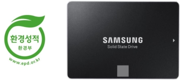
Samsung Electronics SSD, the first semiconductor to receive Environmental Product Declaration (EPD) certification
Samsung Electronics' bestselling SSD (Solid State Drive) model '850 EVO 250GB' has become the first in the semiconductor industry to obtain 'Environmental Product Declaration (EPD)' certification. The 'Environmental Product Declaration,' overseen by the Ministry of Environment and operated by the Korea Environmental Industry and Technology Institute, is a nationally recognized certification system that quantitatively displays and publicly discloses the environmental impact of products and services throughout their entire lifecycle—from raw material extraction through production, transportation and distribution, use, and disposal. It serves as an indicator enabling consumers to select more environmentally friendly products. The '850 EVO 250GB' model has obtained EPD certification for SSD products and will disclose six major environmental performance metrics: ▲resource depletion ▲global warming ▲ozone layer depletion ▲acidification ▲eutrophication ▲photochemical ozone creation potential.
2017.05.23by 김지혜 기자

Intel Unveils Next-Generation 'Core Ultra Series 3' and vPro Platform for Enterprise PCs
Intel has officially unveiled the "Intel Core Ultra Series 3" for next-generation enterprise PCs and the latest vPro platform, addressing a wide range of demands from enterprise notebooks to high-performance workstations.
2026.03.26by 배종인 기자

ROHM Launches ESD Protection Diode Compatible with High-Speed Interfaces of 10Gbps or Higher
Semiconductor specialist ROHM has developed the 'RESDxVx series' of ESD (electrostatic discharge) protection diodes capable of responding to next-generation high-speed data communication environments exceeding 10Gbps, simultaneously enhancing both signal quality maintenance required in high-speed interfaces and IC protection performance.
2026.03.26by 배종인 기자











