


[Interview] FPGA Debugging Tool, This Convenient When Used Properly
 Published2017.06.02 19:16
When designing an FPGA, you must go through the debugging process to check whether the written program is correct and has no errors.
So how can we make debugging easier and faster? Intel's FPGA design software, a debugging tool for correcting errors in FPGAs, provides a satisfactory answer to this question.
This 'Quartus' includes five debug tools: ▶SignalProbe Incremental Routing ▶In-System Memory Content Editor ▶In-System Sources & Probes ▶SignalTap II embedded logic analyzer ▶Logic Analyzer Interface.
First, SignalProbe Incremental Routing helps you connect specific logic cells to external pins without compiling them entirely, so you can check them with a logic analyzer or oscilloscope. In general, in the case of FPGAs, fitting and routing tasks must be performed together because internal resources are used to connect internal signals to the outside. However, the Incremental Routing function can be performed quickly because it connects to the outside using previously unused routing resources. .
Additionally, the 'In-System Memory Content Editor' is used to check and update the contents of the internal memory via JTAG (Joint Test Action Group). ISMCE can modify or update internal memory while the device is running, and it must be connected because it happens through the JTAG controller. The IPs supported by ISMCE are LPM_CONSTANT, single port ROM and RAM.
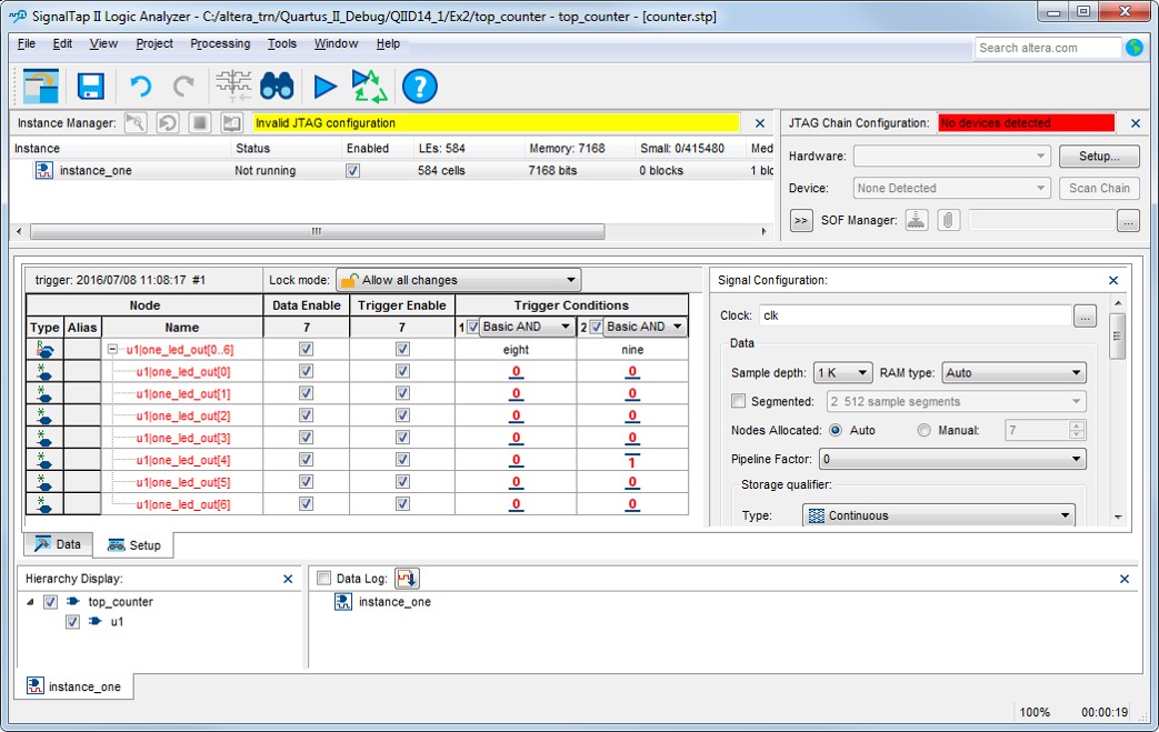
'In-System Sources & Probes' also works via JTAG. Each ISSP can have up to 512 probes and toggles during runtime. In simple function debugging, if an instance of ISSP IP is possible, a connection is absolutely necessary because JTAG is used as a debugging channel, and it can be used in a PC environment without additional external devices.
The function of 'SignalTap II embedded logic analyzer' is to monitor internal signals using predefined clock signals. Various signals can be monitored in real time. Add SignalTap II to the completed custom code, select the target probe point, and set the trigger condition. Then compile the entire code and program the result value to the device. The analysis results can be viewed through the debugging GUI of SignalTap II.
Finally, the 'Logic Analyzer interface' is used to increase visibility of signals inside the FPGA. It connects internal signals to I/O pins and then connects them to external test devices. Up to 256 internal signals can be connected to each pin, and internal probe points can be quickly switched and connected. No need to recompile or reconfigure separately for work.
Intel's Axios FAE Vice President Hyunsoo Jeon said, "Intel's 'Quartus' has an intuitive GUI environment for easy user access. The debugging tool also allows debugging of specialized blocks such as transceivers, including basic internal logic." He added, "When using a debugging tool, it is important to secure the JTAG connection and then use the appropriate tool according to the situation."
A detailed explanation of the Intel Quartus debugging tools and how to use them appropriately for each debugging situation can be found in the online webinar (eeWebinar).
Comments
Related news

Intel, 7th Generation Intel Core Processor with Tuning PC and Overclocking
Intel authorized distributors Intech & Company, PC Direct, and Coeit announced they will conduct a quiz promotion featuring video content showing the process of building a tuning PC and overclocking with the Intel Core i7-7700K processor. The 7th generation Intel Core processors underwent various improvements compared to previous generation models. Notable features include an improved 14nm manufacturing process and operation based on the Intel 200 series chipset, enhanced CPU operational performance, improved memory bandwidth, advanced graphics performance, and improved overclocking success rates.
2017.03.15by 김자영 기자
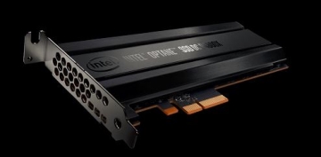
Intel Unveils Fastest Response Speed SSD in Reality
Intel has unveiled the Intel Optane SSD DC P4800X series. This series enhances scalability per server and application speed. By expanding the system memory pool and forming large-capacity, cost-effective memory, it provides users with enhanced insights.
2017.03.21by 김자영 기자
.jpg)
SalePoint Signs Multi-Year Partnership Agreement with AWS… Promoting Identity Security that Integrates Even AI Agents
Sailpoint has entered into a multi-year strategic partnership agreement with AWS and is moving forward with establishing an integrated governance system that manages both human and non-human identities together. The plan is to consistently manage access permissions in an environment where AI agents are increasing as work execution entities, while applying the principle of least privilege and automated policy enforcement. The two companies plan to jointly expand capabilities to manage the identities of various entities, including AI agents, within a single layer in the AWS environment. This collaboration is interpreted as a move to design security and governance together in corporate environments where AI adoption is expanding.
2026.03.26by 배종인 기자
.png)
Databricks Unveils Open AI Security Monitoring 'Lakewatch'
Databricks entered the security market on March 24 by unveiling LakeWatch, an open-source agentic SIEM. The core functionality of this product is to integrate and analyze security, IT, and business data in a single environment to support AI-based threat detection and investigation. The company explained that it reduces the limitations of existing security operations centers, which have had to forgo some data due to high cost structures, and enables large-scale data analysis and automation based on open formats and ecosystems. LakeWatch is currently offered as a private preview, with Adobe and Dropbox mentioned as early customers. Databricks also announced an expanded partnership with Anthropic as well as the acquisition of Antimatter and SiftD.ai.
2026.03.26by 배종인 기자

Ecolab Expands AI Data Center Cooling Business Through Acquisition of CoolIT
Ecolab has agreed to acquire CoolIT Systems, a liquid cooling company for AI data centers, for approximately $4.75 billion. The transaction is expected to close by Q3 2026, subject to regulatory approvals. CoolIT has been supplying direct-to-chip cooling-based coolant distribution units, cold plates, and manifolds, serving hyperscale data centers and colocation operators as customers. This acquisition is a measure to address the high-heat and high-density server environments created by AI proliferation. Ecolab plans to combine its water management and digital monitoring capabilities with CoolIT's hardware technology to expand its data center cooling business.
2026.03.26by 명세환 기자











